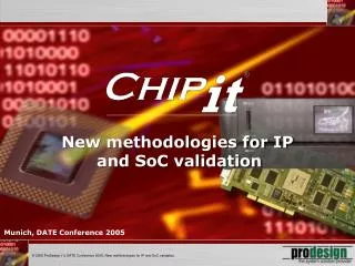
New methodologies for IP and SoC validation
New methodologies for IP and SoC validation. Munich, DATE Conference 2005. ProDesign’s Verification Solutions. New methodologies for IP and SoC validation Patrick Le Mélédo Business Development Manager, ProDesign. Software. IP’s. Memories. SoC. CPU. BUS Systems. IO`s. Interfaces.

New methodologies for IP and SoC validation
E N D
Presentation Transcript
New methodologies for IP and SoC validation Munich, DATE Conference 2005
ProDesign’s Verification Solutions New methodologies for IP and SoC validation Patrick Le Mélédo Business Development Manager, ProDesign
Software IP’s Memories SoC CPU BUS Systems IO`s Interfaces Software Software Controller etc. Software Development of SoC Designs
Development of SoC Designs • There are some problems, which must be solved • External IPs must be implemented (OCP standard socket is helpful) • Complete SoC Design must be verified • SW development needs a “prototype” of the complete SoC ASAP • Multiple “prototypes” for a reasonable price are required • Prototype has to run in higher speed for SW development • Simulation is too slow, that it can be used for SW development • Simulation accelerators and Emulation systems are too expensive • The SoC Design has to be verified in the real environment • Therefore new Methodologies are required !!!
Mixture of all solutions would be the best Verification Methodologies Current Methodologies for Design Verification Simulator Positive: - Very fast compilation of design - 100% Visibility, highest debugging possibilities Negative:- Low speed (kHz) - Design can not be tested in real environment Emulator/Simulator Accelerator Positive:- Short compilation time - High Visibility, good debugging possibilities - Higher speed (up to 1 MHz) Negative:- Expensive - speed is not fast enough in In-Circuit mode Rapid Prototyping Positive:- Highest speed performance (up to 200MHz) - Design can be tested in real environment - Multiple prototypes for software development Negative:- Low debugging possibilities - Long compilation time
Simulation Rapid Prototyping Emulation ProDesign Verification Methodologies CHIPit, the successful mixture
ProDesign Verification Methodologies CHIPit, the individual Verification Solution Gold Edition Silver Edition Platinum Edition • Up to 200 MHz System speed • 2 x Virtex-II 6-/8000 FPGA • Up to 1,1 M ASIC gates • PCI Solution • 1 x Virtex-II 4-/6-/8000 FPGA • Up to 0,55 M ASIC gates • High capacity platform • 3 – 18 Virtex-II, 10 M gates • 3D Switching Technology • Scaleable product portfolio • Hardware assisted verification systems usable in all phases of ASIC and SoC Design • Fastest Rapid Prototyping System on the market (up to 200 MHz) • Only reconfigurable system, which can handle up to 18 FPGAs (10 M ASIC gates) • Integrated Co-Simulation and Debugging Features • more than 100 installed systems worldwide
ProDesign Verification Methodologies CHIPit, the individual Verification Solution Behavior Prototyping One common platform for functional verification Co-Simulation In-Circuit Emulation ASIC Rapid Prototyping Software Development IP & SoC Validation
Testing Phase Tape Out System Integration Concept Phase C, C++ IPs, Design modules Algorithm Creation & Validation RTL Simulation Design Phase Evaluation Phase HW SW Performance Optimization Design Module & IP Creation • Software Development • High volume Replicates • Low cost custom boards developed and manufactured in short time by ProDesign • System Integration • In-Circuit test • Firmware development • First Replication • First time FPGA implementation • IP Debugging • Subsystem Integration • Co-Simulation • Acceleration • Proof of concept • Real world data ProDesign Verification Methodologies CHIPit in the design flow, methodology
Suitable CHIPit system Top level Gold Edition Silver Edition .... IP1 IP2 IP3 IP4 IPn System Integration Platinum/Platinum Plus Edition Software/Firmware Development Custom low cost replicate boards .... Developed, manufactured and tested by Team 1 Team 2 Team 3 Team 4 Team n ProDesign Verification Methodologies CHIPit in the design flow, methodology
Host (PC, Workstation) HDL-Bridge Signal Tracker CAPIM Visibilty Tool Co-Simulation Debugging In-Circuit Debugging C/C++ Interface Co-Simulation/Emulation Interface Probing of Signals Visibility of Signals in Simulator TCL Interface VCS Synopsys NCSIM Cadence ModelSim Mentor Logic-Analyzer Programming Read-, write-, interrupt-, reset-..., functions Simulator Hardware modules Manager Memory DSP Project handling Processor IPs UMRBus UMRBus UMRBus UMRBus UMRBus System Configuration Interfaces LCD others Cust. boards Synthesis Partitioning Optimization ProDesign Verification Methodologies Platinum Edition, the SoC Verification System
Auspy ProDesign Verification Methodologies How to bring the Design into the box RTL Design Compiler FPGA Leonardo XST Synplify Synthesis FPGA Design Partioning Partitioning SRT-Tool FPGA Connection Management Prototype in Hardware
ProDesign Verification Methodologies Speed comparison of different verification modes Verification Performance In-Circuit Transaction based Emulation MHz KHz Co-Simulation Transaction based Simulation Hz Simulation Level of Integration IP Blocks SoC with Software Sub-Systems SoC
Transaction based Emulation Co-Simulation In-Circuit up to 200 MHz Between 10 kHz and 100 KHz Up to 200 MHz Benefit • Good Debug possibilities • Design can be tested in real environment Weakness • Very low speed Benefit • Design can run in high speed • Design can be tested in real environment Weakness • Limited Debug possibilities Benefit • Design can run in high speed • Good debugging possibilities Weakness • Expenses to build transactors ProDesign Verification Methodologies Differences between the verification modes
Customer specific Design IP Block 1 IP Block 2 IP Block 3 IP Block 4 IP Block 5 DUT Standard Modules Memory DSP Processor IPs Interfaces Controller ProDesign Verification Methodologies In Circuit Verification Target System High speed Verification, up to 200 MHz
ProDesign Verification Methodologies Co-Simulation Verification Host (PC or Workstation) • Runs HDL modules in hardware • You can integrate the „real world“ in your simulation • You can use the original testbench • You can run your simulation faster • Verify HDL Modules, IP’s or whole Designsbetween Simulator & CHIPit • One Host with one or multiple CHIPit • Runs through UMRBus communication system • The following simulators are supported: • Synopsys VCS ( Verilog, VHDL) • Mentor Modeltech Modelsim (Verilog, VHDL) - Cadence NCSIM, (Verilog, VHDL) • Supported on all CHIPit Platforms Testbench IP 1 IP 2 IP 3 IP 4 IP 5 Simulator Simulator DUT DUT HDL Bridge Simulator Environment UMRBus CHIPit Platform HDL Bridge Hardware Environment IP 2 IP 4 IP 5 DUT
ProDesign Verification Methodologies • Debugging Possibilities with the CHIPit System • In-Circuit Mode • Probing of internal Signals after the place and route • Debug instrumentation in RTL with third party tools Co-Simulation Mode • Connection of RTL Simulator to Rapid Prototyping System • Signal Tracker captures FPGA register information and showed it in Simulator In-Circuit and Co-Simulation Mode • UMRBus Communication System
ProDesign Verification Methodologies CHIPit Debugging Possibilities (In-Circuit) • Description • Makes internal signals inside the FPGA visible • Routes internal signals to free pins, after synthesis and the place & route • Benefit • Handles multiple debug versions; no new synthesis & place & route necessary • Easy integration and programming of logic analyzer Weakness • Limited number of free pins Visibility Tool Connection UMRBus Logic Analyzer System Host
ProDesign Verification Methodologies Debugging Possibilities (In-Circuit), Third parties • Description • Insert logic into RTL design, before synthesis and place & route • Monitors signals with embedded logic analyzer • Benefit • Higher visibility, to debug design Weakness • RTL Design has to be changed; uses valuable FPGA resources • Synthesis • Partitioning • Place & Route JTAG Embedded Logic Analyzer System Host
ProDesign Verification Methodologies CHIPit Debugging Possibilities (Co-Simulation) • Description • Using the readback functionality of Xilinx Virtex-II FPGAs and captures register information in FPGA, and made it visible in RTL Simulator • Benefit • Full design visibility for optimal debugging • No change of design and design timing Weakness • Speed goes down in Co-Simulation mode Signal Tracker UMRBus UMRBus RTL Simulator System Host
CHIPit Verification Suite High Speed Debug Low Speed Testing and Debug <1Mhz NCSIM Cadence ModelSim Mentor VCS Synopsys RIPV Regression Test Waveform View Visibility Tool for LA HDL-Bridge Signal Tracker Host UMRBus Communication System DLL Linux Windows Solaris Configuration Diagnostic Self-Test DLL C, C++ (System C) Tcl/Tk User Applications Manager ProDesign Verification Methodologies CHIPit UMRBus, let’s talk to hardware
ProDesign Verification Methodologies Example targeting Image Processing Monitor and controldisplay created with Tcl/Tk within Minutes UMRBus CAPIM #1 CAPIM #2 From host Image width Image height Threshold IMG2UMR Threshold Digital oranalog Frame grabber Frame grabber board IMG CAPIM #3 User design To host
Customer Success Stories Sony Semiconductors • Division: Semiconductor Devices Europe • Prototyping System: CHIPit Gold Edition • Project: Development of a ASIC for a Digital TV Set-top Box Off-air Demodulator MPEG2 Decode Hard-wired DSP Logic ADC Test Equip. Digital TV Set-top Box PCB • Hard-wired DSP logic (that implements demodulation algorithm) is targeted to FPGAs in the emulation platform • Daughter board created to implement tuner/ADC functions
Customer Success Stories Sony Semiconductors Customer statement • “With the CHIPit Gold Edition System we could reach the following demands: • Large FPGAs can cope with complex, fast designs • Able to verify algorithm in real-time with real-world signals • Typical simulation: 1.5s of real-time video takes 1.5 hours • Long-term drift took >2hrs of real-time video to show symptom • This problem could not have been found using simulation alone • Reduces amount of simulation required • Customer and senior management demonstration platform • Facilitates joint working between UK and Japanese design teams • Support software could be debugged before final IC was available” Steve Beck, Project Manager at Sony Semicondutors
Customer Success Stories MICRONAS • Division:System Definition Group, Germany • Prototyping System: CHIPit Gold Edition • Project: Development of a TV Chip • Daughter board created to implement AD & DA functions
Customer Success Stories MICRONAS Customer statement • With the CHIPit Gold Edition System we achieved real time view of our • Picture in Picture application for the ASIC: • particularly the real time possibility for verification is important for us • we found a bug, which could not be reproduced by simulation • to fix the bug was a matter of hours • Micronas uses multiple GOLD systems of the Master & Replicate concept “In our actual project we use systems in different countries. This helps us a lot to share the design work and reach the best solution with our team” • “We work closely with ProDesign as a reliable partner for our verification methodology – we started with CHIPit one year ago and it proved to be • a valuable enhancement for our verification strategy.” Markus Schu, Manager System Engineering at Micronas
ProDesign’s Verification Solutions Conclusion • One platform for all phases of ASIC and SoC design verification • Software, Firmware, IP, Hardware, Customer, .. • High performance • high speed up to 100 and 200 MHz possible • Flexibility • scaleable Systems, upgrade possibility • Different verification modes • Co-Simulation/Emulation • Transaction based Emulation • In-Circuit • High visibility for debug • Fast ROI • excellent pricing allows ROI within first project • Excellent support thanks to long term experience with the same technology • ...and all CHIPit Systems are transportable in a suitcase !
ProDesign’s Verification Solutions End Thank you very much for your attention! Come to see us on Booth n°E4100