
Levels in Processor Design
E N D
Presentation Transcript
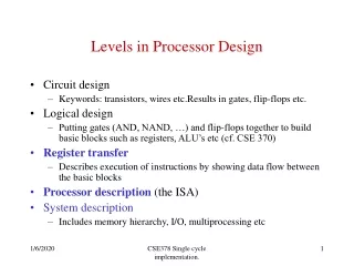
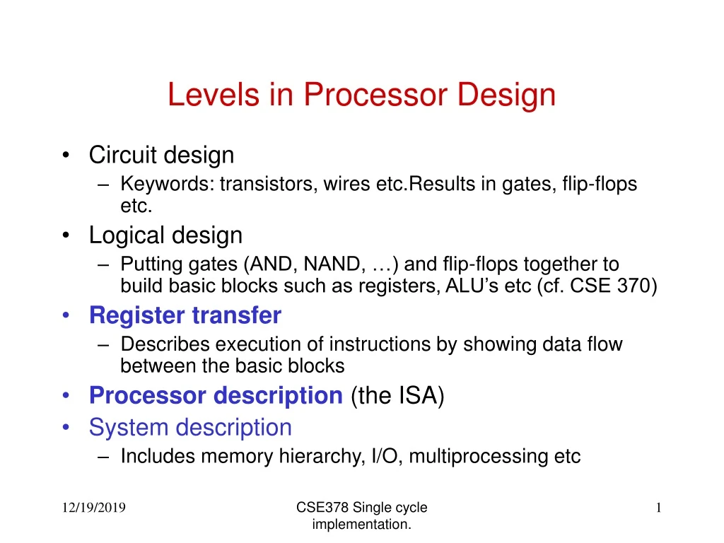
Levels in Processor Design • Circuit design • Keywords: transistors, wires etc.Results in gates, flip-flops etc. • Logical design • Putting gates (AND, NAND, …) and flip-flops together to build basic blocks such as registers, ALU’s etc (cf. CSE 370) • Register transfer • Describes execution of instructions by showing data flow between the basic blocks • Processor description (the ISA) • System description • Includes memory hierarchy, I/O, multiprocessing etc CSE378 Single cycle implementation.
Register transfer level • Two types of components (cf. CSE 370) • Combinational : the output is a function of the input (e.g., adder) • Sequential: state is remembered (e.g., register) CSE378 Single cycle implementation.
Synchronous design • Use of a periodic clock • edge-triggered clocking determines when signals can be read and when the output of circuits is stable • Values in storage elements can be updated only at clock edges • Clock tells when events can occur, e.g., when signals sent by control unit are obeyed in the ALU Storage Elem 1 Storage Elem 2 Note: the same storage element can be read/written in the same cycle Comb.logic Clock cycle CSE378 Single cycle implementation.
Storage Elem 1 Storage Elem 2 Comb.logic Write signal Write signal Logic may need several cycles to propagate values True in designs today with very high clock frequency CSE378 Single cycle implementation.
Processor design: data path and control unit CPU Combinational Memory hierarchy Control ALU PC Registers state Sequential Memory bus Data path CSE378 Single cycle implementation.
Processor design • Data path • How does data flow between various basic blocks • What operations can be performed when data flows • What can be done in one clock cycle • Control unit • Sends signals to data path elements • Tells what data to move, where to move it, what operations are to be performed • Memory hierarchy • Holds program and data CSE378 Single cycle implementation.
Data path basic building blocks. Storage elements • Basic building block (at the RT level) is a register • In our mini-MIPS implementation registers will be 32-bits • A register can be read or written Input bus Register Write enable signal Output bus CSE378 Single cycle implementation.
Register file • Array of registers (32 for the integer registers in MIPS) • ISA tells us that we should be able to: • read 2 registers, write one register in a given instruction (at this point we want one instruction per cycle) • Register file needs to know which registers to read/write Read register number bus 0 Write register number Read register number bus 1 Write enable Read data output bus 0 Write data input bus Register file Read data output bus 1 CSE378 Single cycle implementation.
Memory • Conceptually, like register file but much larger • Can only read one location or write to one location per cycle Read memory address Write memory address Read control signal Write enable Memory Read data bus Write data bus CSE378 Single cycle implementation.
Combinational elements Multiplexor (MUX): selects the value of one of its inputs to be routed to the output Input busses Mux Select control signal Demultiplexor(deMUX or SEL): routes its input to one of its outputs Output bus Output busses Sel Select control signal Input bus CSE378 Single cycle implementation.
Arithmetic and Logic Unit (ALU - combinational) • Computes (arithmetic or logical operation) output from its two inputs Zero result bit Input bus 0 ALU Output bus Input bus 1 ALU control (opcode/function) CSE378 Single cycle implementation.
Putting basic blocks together (skeleton of data path for arith/logical operations) Zero result bit Read register number bus 0 Write register number Read register number bus 1 Write enable Read data 0 ALU Register file Read data 1 ALU control (opcode/function) Write data input bus CSE378 Single cycle implementation.
Introducing instruction fetch Zero result bit Read Reg #0 Read Reg #1 Write Reg # Read data 0 ALU Reg. File Read data 1 ALU control (opcode/function) Write data Instruction address Instr. memory PC CSE378 Single cycle implementation.
PC has to be incremented (assume no branch) 4 Adder Instruction Instruction address Instr. memory PC CSE378 Single cycle implementation.
Load-Store instructions Read enable Instruction Read data 0 Read Reg #0 Read Reg #1 Write Reg # ALU Data memory Reg. File 32-bit Sign ext “store” data 16-bit offset Write enable Data from “load” R/W address CSE378 Single cycle implementation.
Load-Store instructions Read enable Instruction Read data 0 Read Reg #0 Read Reg #1 Write Reg # ALU Read data 1 Data memory Reg. File Sign ext “store” data 16-bit offset 32-bit Write enable Data for result register R/W address Mux CSE378 Single cycle implementation.
Branch data path ALU 4 Sll 2 Addr 32-bit Instruction Inst. memory PC 16-bit Sgn ext CSE378 Single cycle implementation.