Processor Design
Processor Design. ELEC 418 Advanced Digital Systems Dr. Ron Hayne Images Courtesy of Thomson Engineering. 68HC11 Programming Model . Motorola 68HC11 Microcomputer. 68HC11 Instruction Set Table. PIC18F – MPU and Memory. PIC18F4X2 Architecture Block Diagram. MIPS ISA.

Processor Design
E N D
Presentation Transcript
Processor Design ELEC 418 Advanced Digital Systems Dr. Ron Hayne Images Courtesy of Thomson Engineering
68HC11 Programming Model • Motorola 68HC11 Microcomputer 418_09
68HC11 Instruction Set Table 418_09
PIC18F – MPU and Memory 418_09
MIPS ISA • Instruction Set Architecture • 32 General-Purpose Registers (32-bits) • 3 Instruction Formats • R-format (register) • I-format (immediate) • J-format (jump) • 1 Addressing Mode • Base register and signed offset 418_09
MIPS Subset Sequence of Operations Fetch an Instruction Decode the Instruction Execute the Instruction Data Path Design 418_09
Instructional Processor Design • 3 Bus Organization • 16 bit Data Path • 4 Word Register File • 4K Word Memory • 8 Function ALU • 2 Condition Code Flags • 6 Data Instructions • 4 Addressing Modes • 7 Branch Instructions 418_09
Data Path & Memory STACK BUS B BUS C BUS A 12 PC IR A1 A2 1 REGS 2 2 MUX A ALU R B MUX STATUS NZ MDR 12 MAR MEM
ALU Multiplexers BUS A15-5 0's,A10-9 0's,A9-5 1's,A10-9 1's,A9-5 BUS A4-0 BUS B15-5 0's,B10-9 0's,B6-5 BUS B4-0 Branch 0 1 SRC or DST S 0 0 0 1 1 1 Sign S S S 0 1 Address S 0 1 11 5 Extend S ALU B15-5 ALU B4-0 11 5 ALU A15-5 ALU A4-0 418_09
Data Path Registers & Memory • Program Counter (PC) • 12-bit Program Address • Subroutine Stack (STACK) • 16 x 12-bit Addresses • Instruction Register (IR) • 16-bit Instructions • Register File (REGS) • 4 x 16-bit Registers • Arithmetic Logic Unit (ALU) • 8 Functions (ALU_OP) • Flag Register (STATUS) • Negative Flag (N) • Zero Flag (Z) • Memory Data Register (MDR) • 16-bits to/from Memory • Memory Address Reg (MAR) • 12-bit Memory Address • Memory (MEM) • 4K x 16-bit Memory 418_09
Memory Map • 4K (4096) RAM • 8 Memory-mapped I/O Ports • 0x000 Switch (Input) • 0x001 LED (Output) • 120 Data Memory Locations • 0x008 - 0x07F • 3968 Program Memory Locations • 0x080 - 0xFFF 418_09
Addressing Modes • Method of specifying of an operand • Immediate (Literal) addressing • The operand is a number that follows the opcode • Direct (Absolute) addressing • The address of the operand is a part of the instruction • Indirect addressing • An address is specified in a register (pointer) and the MPU looks up the address in that register 418_09
15 14 13 12 11 10 9 8 7 6 5 4 3 2 1 0 OP SRC DST VALUE IR Data Instruction Format EA = Effective Address vv = Upper 2 bits of Value * = SRC only 418_09
Data Instructions 418_09
15 14 13 12 11 10 9 8 7 6 5 4 3 2 1 0 OP MD OFFSET IR Branch Instruction Format 418_09
Assembly Language Program MOVE N,R1 MOVE #NUM1,R2 MOVE #0,R0 LOOP ADD (R2),R0 ADD #1,R2 ADD #-1,R1 BNZ LOOP MOVE R0,SUM STOP BRA STOP 418_09
Control Unit Organization Control Step Counter CLK Step DCD T0 . . . T7 I0 InstructionDCD . . . I7 M0 N SRC_MODEDCD STATUS IR Encoder M3 . . . . . . C M0 DST_MODEDCD M3 . . . Clear Control Signals 418_09
Control Signals • BUS_A • BUS_B • REGS_Read1 • REGS_Read2 • Extend • Address • ALU_Op • MEM_Read • MEM_Write • Inc_PC • Load_PC • Push_PC • Pop_PC • Load_IR • REGS_Write • Load_STATUS • Load_MDR • Load_MAR • Clear 418_09
Control Unit Design • Instruction Fetch 418_09
Control Unit Design • Instruction Execute • MOVE Rs,Rd • Register Direct (M0), Register Direct (M0) 418_09
Control Unit Design • Instruction Execute • MOVE Value,Rd • Immediate (M3), Register Direct (M0) 418_09
Control Unit Design • Instruction Execute • BRA Offset • Branch Always • OP (111), Mode (000) 418_09
VHDL Model (Phase 1) • Data Path • Components • Control Unit • Instruction Fetch • Instruction Execute • First Test Program • program1.asm • program1.bin MOVE #3,R1 MOVE R1,R2 STOP BRA STOP 418_09
VHDL Model (Phase 1) • processor.vhd • processor_components.vhd BUS B BUS C BUS A 12 PC IR A1 A2 1 REGS A1 A2 2 1 REGS 2 2 2 A MUX A ALU R ALU R B B MUX STATUS NZ MDR MEM 12 MAR MEM 418_09
VHDL Testbench constant CLK_period : time := 20 ns; stim_proc : process begin RESET <= '1'; wait for CLK_period*1.25; RESET <= '0'; wait for CLK_period*80; end process; 418_09
VHDL Simulation (Phase 1) 418_09
Control Unit Design (Phase 2) • MOVE Rs,Addr • Register Direct (M0), Absolute (M2) 418_09
Control Unit Design (Phase 2) • MOVE Addr,Rd • Absolute (M2), Register Direct (M0) 418_09
Control Unit Design (Phase 2) • ADD (Rs),Rd • Register Indirect (M1), Register Direct (M0) 418_09
Control Unit Design (Phase 2) • ADD #Value,Rd • Immediate (M3), Register Direct (M0) 418_09
Control Unit Design (Phase 2) • BNZ Offset • Branch if greater than zero • OP (111), Mode (010) 418_09
Assembly Language Program • program2.asm • program2.bin MOVE N,R1 MOVE #NUM1,R2 MOVE #0,R0 LOOP ADD (R2),R0 ADD #1,R2 ADD #-1,R1 BNZ LOOP MOVE R0,SUM STOP BRA STOP 418_09
VHDL Control Unit (Phase 2) • processor.vhd Control Step Counter CLK Step DCD T0 . . . T7 I0 InstructionDCD . . . I7 M0 N SRC_MODEDCD STATUS IR Encoder M3 . . . . . . C M0 DST_MODEDCD M3 . . . Clear Control Signals 418_09
VHDL Simulation (Phase 2) 418_09
Microcontroller (Phase 3) • 4K (4096) RAM • 8 Memory-mapped I/O Ports • 0x000 SWITCH (Input) 8-bit • 0x001 LED (Output) 8-bit • 0x002 ANODE (Output) 4-bit • 0x003 CATHODE (Output) 8-bit • 120 Data Memory Locations • 0x008 - 0x07F 418_09
MEM4K entity MEM4K is port(CLK: in std_logic; MEM_Read: in std_logic; MEM_Write: in std_logic; Addr: in std_logic_vector(11 downto 0); Data_In: in std_logic_vector(15 downto 0); Data_Out: out std_logic_vector(15 downto 0); SWITCH: in std_logic_vector(7 downto 0); LED: out std_logic_vector(7 downto 0); ANODE: out std_logic_vector(3 downto 0); CATHODE: out std_logic_vector(7 downto 0)); end MEM4K; 418_09
15 14 13 12 11 10 9 8 7 6 5 4 3 2 1 0 OP SRC DST VALUE IR Data Instruction Format EA = Effective Address vv = Upper 2 bits of Value * = SRC only 418_09
Data Instructions 418_09
15 14 13 12 11 10 9 8 7 6 5 4 3 2 1 0 OP MD OFFSET IR Branch Instruction Format 418_09
FPGA Implementation Clock Processor LED Reset SWITCH ANODE/CATHODE
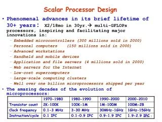
Summary • Example Microprocessors • Instruction Set Architecture • Instructional Processor Design • Data Path • Memory • Instruction Processing • VHDL Model • ISim Simulation • FPGA Implementation 418_09