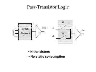
Download
1 / 16
160 likes | 288 Vues
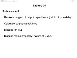
Lecture 24. Today we will Review charging of output capacitance (origin of gate delay) Calculate output capacitance Discuss fan-out Discuss “complementary” nature of CMOS. ORIGIN OF GATE DELAY. When the inputs A and B change such that the output F changes,

E N D
Lecture 24 • Today we will • Review charging of output capacitance (origin of gate delay) • Calculate output capacitance • Discuss fan-out • Discuss “complementary” nature of CMOS
ORIGIN OF GATE DELAY When the inputs A and B change such that the output F changes, the output cannot change instantaneously; the output capacitance must be charged or discharged. VDD S S A PMOS1 PMOS2 F B NMOS1 S NMOS2 S This is GATE DELAY.
REVIEW: PULL-DOWN DEVICES In our logic circuits, the NMOS transistors have • Gate terminal connected to VIN • Source terminal connected to ground directly, or through another NMOS This means • When VIN is high, NMOS transistors are “on”. They help pull-down VOUT to ground, by conducting current to discharge the output capacitance. • When VIN is low, NMOS transistors are “off”. They act as open circuits from source to drain.
REVIEW: PULL-UP DEVICES In our logic circuits, the PMOS transistors have • Gate terminal connected to VIN • Source terminal connected to VDD directly, or through another PMOS This means • When VIN is low, PMOS transistors are “on”. They help pull-up VOUT to VDD, by conducting current to charge the output capacitance. • When VIN is high, PMOS transistors are “off”. They act as open circuits from source to drain.
REVIEW: MODEL FOR GATE DELAY ANALYSIS There is a model for the behavior of transistors in a CMOS logic circuit to analyze charging/discharging of the output capacitance. VIN = 0 (for NMOS) VIN = VDD (for PMOS) VIN = VDD (for NMOS) VIN = 0 (for PMOS) D D The resistance R is the effective resistance for the device during the first half of the transition. Each device can have different R! G G R R S S
REVIEW: CALCULATING EFFECTIVE RESISTANCE Consider pull-down, when VOUT must go from VDD to 0 V. VDD ID(N) t=0 ID(N)≈ IDSAT(N) RP t=tp ID(N) ≈ IDSAT(N) VOUT VDD VDS(N) VDD/2 VDD We calculate RN by averaging the values of VDS(N)/ID(N) at the beginning and ending of delay. RN RP = -¾ VDD / IDSAT(P) RN = ¾ VDD / IDSAT(N)
CALCULATING OUTPUT CAPACITANCE • Two major sources of capacitance: • The transistor gates in the next stage • The metal connection to the next stage Both can be computed using the parallel plate capacitor formula: A is the area of the plates, k is the dielectric constant of the insulator in between the plates, e0 is the permittivity of free space, and d is the distance in between the plates. since this is fixed by fabrication process. We denote
CALCULATING OUTPUT CAPACITANCE Each transistor gate terminal attached to the output contributes a gate capacitance where W and L are the channel dimensions and COX is the capacitance of the gate per unit area (parameters from ID vs. VDS). Each metal connection at the output contributes a capacitance also given by the parallel plate capacitor formula, but with different length, width, and capacitance per unit area.
EXAMPLE VDD VDD S S S VOUT1 VOUT2 VIN S S S Suppose that VIN was logic 1 for a long time, and then switches to logic 0 at t = 0. Find the propagation delay through the inverter.
EXAMPLE Use VDD = 5 V VTH(N) = -VTH(P) = 1 V COX = 5 fF/µm2 for both transistors L = 2 µm for both transistors W = 2 µm for both transistors l = 0 for both transistors µN= 50000 mm2 / (V s) µP= 25000 mm2 / (V s) WI = 2 µm LI = 200 µm COX(I) = 0.1 fF/µm2 Calculate the effective resistance and total output capacitance due to gate and interconnect capacitance.
EXAMPLE Since VIN is now low, VOUT1 must go from low to high. Pull-up VDD RP VDD S VOUT VDD VIN = 0 V RN S RP is the resistance involved in the charging.
EXAMPLE RP = - ¾ VDD / IDSAT(P) RP = - ¾ (5 V)/ (W/L mP COX (VGS(P) – VTH(P))2 ) RP = - ¾ (5 V)/ (2mm/2mm 25000 mm2/Vs 5 fF/mm2 (-5 V – -1V)2 ) RP = 1.875 kW Now calculate COUT: There are 4 transistor gates attached to inverter output, and one wire connecting the inverter output to the NAND input. COUT = 4 CG + CI
EXAMPLE CG = W L COX = (2 mm)(2 mm)(5 fF/mm2) = 20 fF CI = WI LI COX(I) = (2 mm)(200 mm)(0.1 fF/mm2) = 40 fF COUT = 4 CG + CI = (4)20 fF + 40 fF = 100 fF tP = 0.69 RP COUT = 0.69 (1.875 kW) (100 fF) = 129 ps
FAN-OUT Consider our previous example. Suppose that we connected N NAND gates to the output of the inverter. Each NAND gate adds 4 more gate capacitances and another interconnect capacitance. COUT = N(4 CG + CI) = 100 N fF tp = 129 N ps The fan-out, or number of logic gates that can be attached to an output, is limited by propagation delay considerations.
LOOKING AT CMOS CIRCUITS One can often “see” the logical operation in a CMOS circuit by looking at either the top or bottom half of the circuit. VDD A C B For example, looking at the top half of this circuit, we see that the output will be connected to VDD (F is high) when: (B OR C is low) AND A is low F = (B + C) A F B A C
LOOKING AT CMOS CIRCUITS The bottom half of the circuit always results in the same equation as the top half, just rewritten via DeMorgan (that’s why output is always defined). VDD A Looking at the bottom half of this circuit, we see that the output will be connected to ground (F is low) when: (B AND C are high) OR A is high F = B C + A F = B C + A C B F B A C