Download
1 / 60
670 likes | 1.14k Vues
Scanning probe microscopy (SPM) and lithography. Scanning tunneling microscopy. Piezoelectric positioning. Atomic force microscopy (AFM) overview. AFM tip and its fabrication. Tapping mode AFM. Other forms of AFM (LFM, EFM, MFM, SCM…).

E N D
Scanning probe microscopy (SPM) and lithography Scanning tunneling microscopy. Piezoelectric positioning. Atomic force microscopy (AFM) overview. AFM tip and its fabrication. Tapping mode AFM. Other forms of AFM (LFM, EFM, MFM, SCM…) “Scanning probe microscopy and spectroscopy” by Roland Wiesendanger is a good comprehensive reference book. It can be found at (read only, no download): http://books.google.ca/books?id=EXae0pjS2vwC&pg=PA561&lpg=PA561&dq=liquid-metal-covered+tungsten+needle&source=bl&ots=Yy9A2saE3M&sig=KIDbgh_HQLg4LQPA4XIVh7TD3kQ&hl=en&ei=4cdkSsjqMYLWtgOX_ehm&sa=X&oi=book_result&ct=result&resnum=1 ECE 730: Fabrication in the nanoscale: principles, technology and applications Instructor: Bo Cui, ECE, University of Waterloo; http://ece.uwaterloo.ca/~bcui/ Textbook: Nanofabrication: principles, capabilities and limits, by Zheng Cui
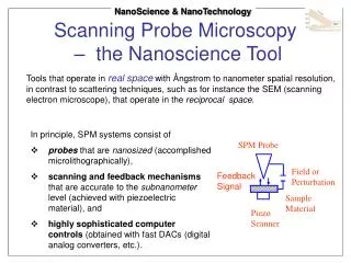
Scanning probe microscopy (SPM) overview • Normally used for characterization of topographic, physical and chemical properties, though they can also be used as a lithography tool with high resolution yet low throughput. • For imaging purpose, compared to SEM: • Extremely accurate in the z-dimension (<<1Å); whereas for SEM to see the vertical cross-section profile one has to cut the sample and tilt it, and the resolution is much worse than 1nm. • For lateral (xy-) dimension, SPM is accurate only when the surface is relatively flat, then the resolution is better than SEM (atomic resolution for SPM vs. few nm resolution for SEM). • For non-flat surface, there are often artifacts for SPM imaging because the tip is not infinitely thin and long. As a result, a vertical profile always appears slopped when imaged using SPM. • AFM generally don’t need vacuum and can image any surface (insulator or not) and even inside liquid (very important for bio-imaging). • AFM is much cheaper than high resolution field emission SEM and is thus more available (>10 AFMs on campus).
Scanning probe microscopy (SPM) family • Scanning Tunneling Microscopy(STM): topography, local DOS (density of state) • Atomic Force Microscopy (AFM): topography, force measurement • Lateral Force Microscopy (LFM): friction • Magnetic Force Microscopy (MFM): magnetism • Electrostatic Force Microscopy (EFM): charge distribution • Nearfield Scanning Optical Microscopy (NSOM): optical properties • Scanning Capacitance Microscopy (SCM): dielectric constant, doping • Scanning Thermal Microscopy (SThM): temperature, conductivity • Spin-polarized STM (SP-STM): spin structure • Scanning Electro-chemical Microscopy (SECM): electro-chemistry • Scanning Tunneling Potentiometry: surface potential • Photon Emission STM (PESTM): chemical identification
The first STM Instrumentation Exact copy of first Scanning Tunneling Microscope of Binnig and Rohrer STM inventors Rohrer and Binnig, IBM, Zurich, Nobel Prize in Physics in 1986.
Two basic scanning modes • Feedback off/constant height: Scan over surface with constant z0 (piezo voltage), control signal changes with tip-surface separation. For relative smooth surface, faster. • Feedback on/constant current: circuit regulates z piezo voltage to constant value of control signal (constantly changes tip-surface separation). Irregular surfaces with high precision, slower. Constant current STM image corresponds to a surface of constant density of state.
Quantum mechanical tunneling • A voltage applied between two conducting bodies leads to an electrical current even if the two bodies not quite touch: the tunneling current • Interaction: (tunneling-) current (down to pA) • Atomic scale surface topography of electrical conductors • Electronic properties of the surface (“conductivity”) • The tunneling current is strongly dependent on the distance of the two bodies: 1Å changes the current by a factor of 10! Atom Surface STM
Quantum mechanical tunneling Tunneling through a rectangular barrier Elastic tunneling vs. inelastic tunneling Elastic: energy of tunneling electrons conserved. Inelastic: electron loses a quantum of energy within the tunneling barrier.
Tip is the key • The resolution is determined by: • Dimension of probe • Distance of probe to sample Oxide or insulating contamination layers of thickness several nanometers can prevent vacuum tunneling. This may lead to mechanical contact between tip and sample. (the servo will force the tip to collide in an effort to achieve the set-point current) Tunneling through the oxide or contamination layer may damage tip.
STM tip preparation • How to make sharp STM tips? • Wire of W or Pt-Ir, with 200m diameter. • Cut or etch to 40nm diameter tip. • Hand-made, no micro-fabrication process. • Can be sharpened by focused ion beam milling. Very sharp tips can be obtained, ideally terminated by a single atom.
Applications of STM Surface structure with atomic resolution • Surface geometry • Molecular structure • Local electronic structure • Local spin structure • Single molecular vibration • Electronic transport • Nano-fabrication • Atom manipulation • Nano-chemical reaction Various reconstructions of Ge(100)-2x1
Scanning probe microscopy (SPM) and lithography Scanning tunneling microscopy. Piezoelectric positioning. Atomic force microscopy (AFM) overview. AFM tip and its fabrication. Tapping mode AFM. Other forms of AFM (LFM, EFM, MFM, SCM…)
Piezoelectric tube scanner Displacement electric field
Piezo driving technology: the basics Piezoelectric effect: changing the size of an object results in a voltage generated by the object. Inverse piezoelectric effect Discovered in 1880 by Pierre and Jacques Curie Most common material: PZT PZT: Lead zirconium titanate • Piezoelectric materials have an asymmetric unit cell like a dipole. • If these crystals are grown in the presence of a strong electric field then the crystal grains will align and the piezoelectric effect is created. • Typical achievable strain ratio: 1/1000, e.g. 1μm stroke for 1mm PZT.
Unit cell with dipole The central atom is displaced resulting in a unit cell with a dipole moment. Cubic T > Tc Tetragonal T < Tc Tc is Curie temperature, above which the material becomes para-electric (no longer ferroelectric, no dipole moment at the absence of external electric field).
Ferro-electricity (analog to ferromagnetism) Domain structure, hysteresis, coercivity, Curie temperature…
Piezo-ceramics drawbacks Non-linear • Nonlinearity • Creep • Hysteresis • Aging Hysteresis Creep
Relation of ferroelectricity and piezoelectricity The most widely used piezoelectric device is quartz watch. Another confusing phenomenon is piezo-resistive effect, which only causes a change in resistance, without producing an electric potential. Most popular material is single crystal Si.
Scanning probe microscopy (SPM) and lithography Scanning tunneling microscopy. Piezoelectric positioning. Atomic force microscopy (AFM) overview. AFM tip and its fabrication. Tapping mode AFM. Other forms of AFM (LFM, EFM, MFM, SCM…)
Digital Instruments (DI, now Veeco) multi-mode head, scanner and base For DI multi-mode head, sample is put on piezo stage. For DI dimension 3000 head, tip is put on piezo stage.
Probe-sample interaction and detection system Forces and their range of influence
Probe-sample interaction detection system Detect deflection in z-direction (to maintain constant force for normal AFM operation) Detect defection in the x-y direction, for lateral force/friction microscopy. Measure (A+B-C-D)/(A+B+C+D) Measure (A+C-B-D)/(A+B+C+D) Photo-diode (divided into four parts)
Feedback loop for constant force AFM Z is equivalent to the topography of the sample Photo-diode (divided into four parts) Tiny deflection of cantilever leads to large shift of the beam spot position on the photo-diode, so extremely sensitive for z-dimension detection (sensitivity Z << 1Å)
Interactions between sample and tip in force microscopy Far (50-100nm) Close (<10nm) Contact Contact
Force vs. distance AFM can also be used for nano-indentation study to investigate mechanical properties (stress-strain curve, Young’s modulus) of the sample, though force is not as accurate as dedicated nano-indentation tools.
Atomic Force Microscope (AFM) Two basic AFM Modes: Contact mode (no vibrating tip) Tapping mode (vibrating tip) Many variations on Scanning Force Microscopy: Liquid AFM Magnetic Force Microscopy (MFM) Latteral Force Microscopy (LFM) Intermitant and non-contact AFM Force Modulation Microscopy (FMM) Electrostatic Force Microscopy (EFM) Sample: conductor, nonconductor, etc Force sensor: cantilever Deflection detection: photodiode Here tip on piezo-stage, also possible sample on piezo-stage.
AFM mode of operation Intermittent contact and thermal scanning are less popular.
Scanning probe microscopy (SPM) and lithography Scanning tunneling microscopy. Piezoelectric positioning. Atomic force microscopy (AFM) overview. AFM tip and its fabrication. Tapping mode AFM. Other forms of AFM (LFM, EFM, MFM, SCM…)
AFM tip fabrication 1. SiO2 mask 2. RIE Si dry-etch 3. KOH Si wet-etch 4. SiO2 mask 5. RIE Si dry-etch 6. SiO2 mask on backside 7. KOH Si wet-etch, passivation on front-side 8. BHF (buffered HF) SiO2 wet-etch 9. RIE Si dry-etch 10. Release of cantilever in BHF T. Wakayama, T. Kobayashi, N. Iwata, N. Tanifuji, Y. Matsuda, and S. Yamada, Sensors and Actuators a-Physical, vol. 126, pp. 159-164, 2006.
AFM tip fabrication Use EDP instead of KOH. Add oxidation sharpening. EDP: ethylene-diamine pyrocatechol, is an anisotropic etchant solution for silicon, consisting of ethylene-diamine, pyrocatechol, pyrazine and water. Ethylene-diamine Pyrocatechol Pyrazine
Cantilever fabrication – silicon micro-machined probe KOH etch Silicon nitride This type of tip is for contact mode AFM.
Polymer SU-8 tip fabrication KOH etched Si-mould Released tip Spikes
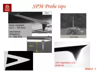
Probe (tip, cantilever) summary Tip array for fast lithography tip for tapping mode AFM tip for contact mode AFM
Electron beam deposited super tip Standard silicon nitirde pyramidal tips which are available commercially are not always sharp enough for some experiments. By focusing the electron beam in a scanning electron microscope onto the apex of the unmodified pyramid tip, a sharp spike of any desired length can be grown. (i.e. growth of carbon from contamination by focused electron beam induced deposition, not necessarily very sharp, but with very high aspect ratio to reach deep holes/trenches.)
Using carbon nanotube to improve resolution Vibration problem: need short tube 0.2m
Scanning probe microscopy (SPM) and lithography Scanning tunneling microscopy. Piezoelectric positioning. Atomic force microscopy (AFM) overview. AFM tip and its fabrication. Tapping mode AFM. Other forms of AFM (LFM, EFM, MFM…)
Scanning modes of AFM 50nm Not popular Vibration 10-100nm
Vibrating cantilever (tapping) mode: most popular • Vibration of cantilever around its resonance frequency (often hundreds of kHz) • Change of frequency due to interaction between sample and cantilever Resonance frequency: keff = k0 - dF/dz (F is force) feff = (1/2π)(keff /m)1/2 Cantilever oscillate and is positioned above the surface so that it only taps the surface for a very small fraction of its oscillation period. When imaging poorly immobilized or soft samples, tapping mode may be a far better choice than contact mode. But for the AFM we have, we operate at 0300kHz
Vibrating cantilever (tapping) mode • Cantilever oscillates at resonant frequency and “taps” sample surface, where feedback loop maintains constant oscillation amplitude. • Reduces normal (vertical) forces and shear (lateral) forces, thereby reducing damage to softer samples, and less tip wear. • Can image surface with weak adhesion. • But much slower than contact mode. Free oscillation Large amplitude Hitting surface Lower amplitude Amplitude imaging (for AFM) Phase imaging (also for MFM and EFM)
Phase imaging • Measure the phase lag of the cantilever driving vs. actual oscillation. • Contrast depends on the physical properties (Young’s modulus…) of the material. Polymer blend (Polypropylene & EDPM) Drive signal Cantilever signal Topography Phase Measure relative elastic properties of complex samples
Atomic resolution AFM AFM (contact mode): Au(111) polycrystalline film on a glass substrate AFM (non-contact mode): Atomic resolution on Si(111) 7x7
Applications to biological system Many types: DNA and RNA analysis, protein-nucleic acid complexes, chromosomes, cellular membranes, proteins and peptides, molecular crystals, polymers and biomaterials, ligand-receptor binding. Bio-samples have been investigated on lysine-coated glass and mica substrate, and in buffer solution (SEM… all in vacuum). By using phase imaging technique one can distinguish the different components of the cell membranes.
Scanning probe microscopy (SPM) and lithography Scanning tunneling microscopy. Piezoelectric positioning. Atomic force microscopy (AFM) overview. AFM tip and its fabrication. Tapping mode AFM. Other forms of AFM (LFM, EFM, MFM, SCM…)
Conductive AFM • Conductive AFM is used for collecting simultaneous topography imaging and current imaging. • Variations in surface conductivitycan be distinguished using this mode. • Cantilever deflection is used as feedback. • Otherwise, for regular STM using tunneling current as feedback, low substrate conductivity may damage the tip. • Now the tunneling current is measured, even though the substrate is an insulator (then no tunneling current). • Standard conductive AFM operates in contact AFM mode. Some AFM tools can be used as STM (no vacuum), with a regular STM W-tip.
Non-contact mode for conductive AFM Torsional resonance mode: keep the tip close to the substrate surface (near field) for tunneling current measurement, with less substrate and tip wear than contact mode. Lateral forces that act on the tip cause a change in the torsional resonant frequency, amplitude, and/or phase of the cantilever, which can be used as feedback to maintain near-field distance.