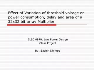
Delay FPGA I/O
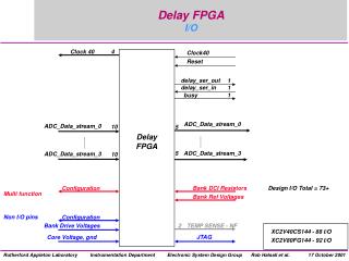
Delay FPGA I/O. Clock 40. 4. Clock40. Reset. delay_ser_out. 1. delay_ser_in. 1. busy. 1. ADC_Data_stream_0. ADC_Data_stream_0. 10. 5. Delay FPGA. 5. ADC_Data_stream_3. ADC_Data_stream_3. 10. Bank DCI Resistors. Design I/O Total = 73+. Configuration. Multi function.

Delay FPGA I/O
E N D
Presentation Transcript
Delay FPGAI/O Clock 40 4 Clock40 Reset delay_ser_out 1 delay_ser_in 1 busy 1 ADC_Data_stream_0 ADC_Data_stream_0 10 5 Delay FPGA 5 ADC_Data_stream_3 ADC_Data_stream_3 10 Bank DCI Resistors Design I/O Total = 73+ Configuration Multi function Bank Ref Voltages Non I/O pins Configuration Bank Drive Voltages 2 TEMP SENSE - NF XC2V40CS144 - 88 I/O JTAG Core Voltage, gnd XC2V80FG144 - 92 I/O
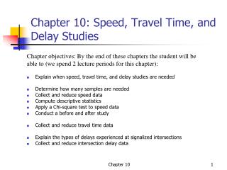
Delay FPGAFunction 4 phases XC2V40-CS144 CLOCK OUT 0 CLOCK - 40 MHz DCM 0 IOB IOB 5 Slices 5 Slices REG DCI 1 10 SHIFT REG REG DATA OUT 0 REG REG BLOCK RAM 0 10 Slices DPM Counter 2.5/3.3V I/O? 4 phases 1.5/1.8/2.5/3.3V I/O? CLOCK OUT 3 DCM 3 IOB IOB 5 Slices 5 Slices REG DCI 4 10 10 SHIFT REG DATA OUT 3 REG REG REG BLOCK RAM 3 10 Slices DPM Control Counter Clock RESET Serial In CONTROL Serial Out busy
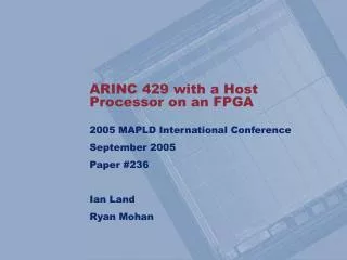
CMS Tracker FED - Front End FPGA Floorplan Die Package Channel 0 FE-BE I/O ADC_Data Channel 3 Delay - Opto - ADC XC2V40CS144 - 88 I/O Clocks XC2V80CS144 - 92 I/O XC2V250CS144 - 92 I/O