Altera vs. Xilinx
Ognjen Šć eki ć. prof. dr Veljko Milutinovi ć. ogi@cg.yu. vm @ etf . bg.ac. yu. Altera vs. Xilinx. Introduction. FPGA vs. ASIC. FPGA = F ield P rogrammable G ate A rray flexibility of software + speed of hardware. ASIC = A pplication S pecific I ntegrated C ircuits

Altera vs. Xilinx
E N D
Presentation Transcript
Ognjen Šćekić prof. dr Veljko Milutinović ogi@cg.yu vm@etf.bg.ac.yu Altera vs. Xilinx Ognjen Šćekić
Introduction Ognjen Šćekić
FPGA vs. ASIC FPGA= Field Programmable Gate Array flexibility of software + speed of hardware ASIC= Application Specific Integrated Circuits tailor-made on demand for specific applications Ognjen Šćekić
Key players: Xilinx, Altera, Lattice, Actel PLD market estimated at $57 billion and rapidly growing The goal is to expand the market: by lowering per-unit cost to attack the low-end market by increasing speed capabilities to attack the high-end market Market Overview Figure 1 - PLD market share Ognjen Šćekić
Pronounced "zylinks" Founded in 1984 Employs around 2,600 people. Claims more than half the world demand for FPGAs. Partners with leading semiconductor manufacturers such as IBM Microelectronics, UMC and Seiko. Xilinx is the net market leader at the moment About Xilinx Ognjen Šćekić
Founded in 1983. Introduced look-up table based architecture in 1992 Second greatest FPGA manufacturer Strategic partner is TSMC About Altera Ognjen Šćekić
Recent FPGA Design Timeline • Virtex and Stratix families are direct opponents, as are Spartan and Cyclone Ognjen Šćekić
• Fabrication process • Logic density • Clock management • On-chip memory • DSP capabilities • I/O compatibility • Software support & other design services Key Factors For ComparingFPGAs Ognjen Šćekić
More advanced fabrication process brings higher integration and thus higher density and/or reduced size of chip. Currently the most advanced is 90nm process (previously 0.13μm) Fabrication Process • first used in Spartan-3, and later in Virtex-4 FPGA family • gave Xilinx one year lead over Altera • Altera introduced it in 2004 with Cyclone II and Stratix II Figure 2 - Cyclone II 90nm structure Ognjen Šćekić
We need a unit to express the logic capability of FPGA Is it possible to define such unit precisely? Traditionally: Xilinx: LC – Logic Cell Altera: LE – Logic Element Logic Density 1 LC = 4-input LUT + D-FF + arithmetic/logic/register circuitry 1 LC = 1 LE Ognjen Šćekić
Improved functionality of "new" architectures introduced new terms: ALM – Adaptive Logic Module for describing Altera's Stratix II family's adaptable structure CLB – Configurable Logic Block for describing Xilinx's FPGA families ELC – Equivalent Logic Cell Xilinx's new unit to better express logic density Logic Density (2) 1 ELC = 1.125 LC 1 CLB has 8 LCs Ognjen Šćekić
Clock management comprises two basic functions: • remove clock skew and propagation delay • generate new clock signals with different frequencies and/or phases Clock Management • All parts of a digital circuit need to be synchronized to a desired clock signal. • If a circuit is large, complex, and operating at high frequencies • the clock propagation delay and clock skew have a great impact on performance. • Therefore, providing a clock signal with zero-delay in all parts of an FPGA • becomes crucial. • The solution is to divide FPGA into regions that can work at different frequencies, • called clock domains. Ognjen Šćekić
It can be done using: DLLs – Delay-Locked Loops (Xilinx) PLLs – Phase-Locked Loops (Altera) Removing Clock Skew Figure 3a - DLL block diagram Figure 3b - PLL block diagram They both compensate for the delay generated on the routing network inside the FPGA, providing zero-delay clock signal to different parts of FPGA. Ognjen Šćekić
Delay-Locked Loop DLL works by inserting delay between the input clock and the feedback clock until the two rising edges align, putting the two clocks in phase. When the two clocks are in phase, the DLL "locks". Thus, the DLL output clock compensates for the delay in the clock distribution network. • Delay-line produces a delayed version of the input clock CLKIN. • Clock distribution network routes the clock to FPGA interior • and to the feedback CLKFB pin. • Control logic sample the input clock and the feedback clock • in order to adjust the delay line. • Delay-line consists on an array of delay elements, • typically CMOS voltage-controlled inverters connected in series. Ognjen Šćekić
Phase-Locked Loop • Instead of a delay line, the PLL uses a voltage controlled oscillator • which generates a clock signal that approximates the input clock CLKIN. • Control logic, consisting of a phase detector and filter, • adjusts the oscillator frequency and phase to compensate for the clock distribution delay. • When the clocks are aligned the PLL "locks". Ognjen Šćekić
PLL DLL PLL vs. DLL Drawback: oscillator accumulates phase error Advantage: does not accumulate phase error Advantage: frequency synthesis is easier because of oscillator Drawback: frequency synthesis is more difficult Altera uses PLLs and Xilinx uses DLLs. Ognjen Šćekić
Beside clock skew elimination, DLLs (PLLs) are also used for: Clock managers need to be resistant to temperature/voltage variations. Clock Generation & Phase Shifting • frequency multiplication and division • duty-cycle regulation • phase shifting Clock manipulation dramatically simplifies the design and improves performance. At the same time it provides many design alternatives. Ognjen Šćekić
Using LUTs as registers does not provide enough space or versatility. Time-dependent applications, performing many computations, need an entire built-in memory. The main advantages of embedded (built-in) memory are: Embedded Memory • short access time • high bandwidth • great versatility • It can behave like: • RAM • ROM • Buffer (FIFO, LIFO, etc.) • Cache • Shift registers • etc… Ognjen Šćekić
DSP– Digital Signal Processing DSP Capabilities • Majority of FPGA applications require some sort of DSP. • In order to increase efficiency DSP computations are executed in parallel - pipelining. • Special DSP units have been developed to fully exploit FPGA's adaptable structure. • These units are designed to optimize execution of commonly used DSP algorithms: • filtering, encoding/decoding, equalization, modulation, FFT, etc • They usually contain: • multipliers (in parallel), accumulators, adders and shift registers Ognjen Šćekić
As FPGAs continue to grow in size and capacity more complex systems are designed for them,demanding an increased variety of I/O standards . Furthermore, as system-clock speeds continue to increase, the need for high-performance I/O becomes more important. Modern bus applications, pioneered by the most influential companies, are commonly introduced with a new I/O standard, tailored specifically to the needs of that application. I/O Compatibility The bus I/O standards provide specifications to other vendors who create products designed to interface with these applications. Each standard often has its own specifications for: current, voltage, I/O buffering and termination techniques. Ognjen Šćekić
Interfaces are implemented in I/O blocks. I/O blocks are parts of FPGA architecture positioned peripherally, connected to I/O pins and to internal interconnects. I/O blocks are grouped into banks – a group of neighboring pins which use the same or compatible I/O standard at the same time. I/O Compatibility (2) Ognjen Šćekić
An I/O block usually contains: I/O Compatibility (3) • programmable I/O buffers • Programmable so they could adjust to different I/O standards. • D-FFs • Used as optional delay elements or registers. • pull-up/down resistors • Used to assert or de-assert pins that would otherwise float. • delay array • Provides a programmable delay of I/O signals. • keeper circuit • Keeps the last state on a bus if all other drivers are in High-Z state. Ognjen Šćekić
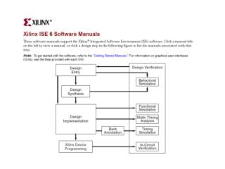
Development of an FPGA-based hardware system can be divided into following stages: system design & synthesis design implementation on-chip verification Software Support Figure 4a - Altera design flow diagram Figure 4b - Xilinx design flow diagram Ognjen Šćekić
Begins with the design entry phase using: HDL – Hardware Description Language (like VHDL or Verilog) schematic editor Software solutions offer complete integrated environments for this stage. A wide variety of FPGA-ready component libraries are available ranging from simple processors, peripheral components, controllers, down to general logic (gates, counters, decoders, etc). Software support hierarchical design entry. System Design Stage Ognjen Šćekić
Once the hardware design is complete it is synthesized: A process that transforms it from HDL form into a low-level gate form, called RTL – Register Transfer Level description. The system design stage is platform independent. The resulting RTL description of our system can be fitted into any FPGA. System Design Stage (2) Figure 5 - HDL and schematic representation of a BCD counter Ognjen Šćekić
Commonly called Place-And-Route stage. Place-And-Route tools take the input RTL netlist for the design and map the logic into the architectural resources of the FPGA. Then, the best location for these blocks is found, based on their interconnections and desired performance. Finally, the interconnects are routed, and pins assigned. Design Implementation Stage Ognjen Šćekić
This stage is platform-dependent, since our design is implemented in an actual FPGA architecture. Therefore, place-and-route tools are developed by the FPGA vendors. They are developed to take full advantage of FPGA architecture, and to provide optimum performance for a given design. Many analysis and simulation tools are provided for this stage. Design Implementation Stage (2) The result of this stage is a configuration file which is loaded into FPGA at startup Ognjen Šćekić
This stage is executed once the design has been loaded into the FPGA. It gives the developer the possibility for real-world debugging. Special cables are supplied with FPGA development kits, for connecting FPGAs to a PC or a workstation. This provides means for reading contents of internal registersand memory. On-Chip Verification Stage Ognjen Šćekić
Software Support (2) • Both Xilinx and Altera offer complete software development kits that guide users through all 3 stages of system design. • Altera offers Quartus II • Xilinx offers ISE • Third-party software tools can be used in system design stage as well. Ognjen Šćekić
Complete designs of some complex systems, written in HDL by FPGA manufacturers, optimized to run on their FPGAs. e.g. microcontrollers, microprocessors, etc. CPUs: Altera: 32-bitNios II Xilinx: 32-bitMicroBlaze "Intellectual Property" Blocks Figure 6 - Block diagram of Altera's 16-bit Nios processor Ognjen Šćekić
When FPGA based designs move in volume production the main issue is cost reduction! Xilinx and Altera have different approaches: Volume Production Solutions Xilinx offers specialized EasyPath FPGAs: Once the clients have developed their system on FPGA, they send it to Xilinx. After 8 weeks they get back the optimized FPGAs with exactly the same functionality. These optimized FPGAs are 30%-80% less expensive when mass produced, and they represent replacements for structured ASICs, and take less time to be completed. Altera offers a service called HardCopy : It is a migration path from the FPGA to structured ASIC. Altera developed a fine-grained cell structure (HCells) ASICs which perfectly match the logic elements (LEs) of Altera’s FPGAs. That way Stratix LEs are mapped to equivalent logic elements in the corresponding HardCopy device. If a Stratix LE is not used in the FPGA design, then it is not mapped to the HardCopy device, yielding a more efficient mapping of the prototyped design. Ognjen Šćekić
Overviews & Comparisons Ognjen Šćekić
low-end FPGA family Ognjen Šćekić
Overview • Most recent Altera's low-end FPGA family • Introduced in 2004, first shipped in February 2005 • 1.2V core, 90nm process Ognjen Šćekić
Packaging • Commercial grade and industrial grade devices are offered. Ognjen Šćekić
Functional Description • Two-dimensional row/column-based architecture to implement custom logic. • Column and row interconnects of varying speeds provide signal interconnects between Logic Array Blocks (LABs), embedded memory, and multipliers. • Logic array consists of LABs, with 16logic elements (LEs) in each LAB. Ognjen Šćekić
Functional Description (2) • Density from 4,608 to 68,416 LEs. • Up to four phase-locked-loops (PLLs). • Global clock network consists of up to 16 global clock lines that drive throughout the entire device. Ognjen Šćekić
Functional Description (3) • M4K memory blocks are true dual-port memory blocks with 4K bits of memory. • Works at up to 260 MHz. • These blocks are arranged in columns across the device in between certain LABs. • Cyclone II devices offer between 119 to 1,152 Kbits of embedded memory. Ognjen Šćekić
Functional Description (4) • Each embedded multiplier block can implement either two 9×9-bit multipliers, or one 18 × 18-bit multiplier. • Embedded multipliers are arranged in columns across the device. • Up to 250-MHz performance. Ognjen Šćekić
Functional Description (5) • Each I/O pin is fed by an IOE (Input Output Element) located at the periphery of the device. • I/O pins support various single-ended and differential I/O standards. • Each IOE contains a bidirectional I/O buffer and three registersfor registering input, output, and output-enable signals. Ognjen Šćekić
Programmable register. Can be configured like D, T, JK or SR flipflop. Used optionally. LE Unit 4-input LUT acts as a function generator for logic functions with 4 variables, or a 16-bit register. Carry logic • Cyclone II LE can operate in 2 modes: • normal mode • arithmetic mode Ognjen Šćekić
LE – Normal Mode • Suitable for general logic applications and combinatorial functions. Ognjen Šćekić
LE – Arithmetic Mode • Implements a 2-bit full adder and basic carry chain Ognjen Šćekić
Column Interconnect.Connects multiple LABs LABs and Interconnects Logic Array Blockconsists of 16 LEs connected with carry and register chains • LAB - Logic Array Block Local Interconnect.Transfers signals between LEs in the same LAB Row Interconnect.Connects multiple LABs Ognjen Šćekić
Clock Management • Clock network features: • Up to 16 Global Clock Networks • Up to 4 PLLs • Dynamic clock source selection, enable and disable • Global clock networks spread throughout the entire device. • They provide clocks for all resources within the device, such as IOEs, LEs, memory blocks, and embedded multipliers. • They are driven by external clock sources (via clock pins),PLL outputs or the logic array signals. • Global clock lines can also be used for general purpose control signals. Ognjen Šćekić
Clock Management (2) • There is one clock control block for each global clock network. • They are arranged on the device periphery. • Clock control blocks are used to select/enable/disable a global clock network. • Multiplexers are used with these clocks to form 6-bit buses to feed LABs and IOEs. Ognjen Šćekić
Clock Management (3) • PLLs are located at the corners: Ognjen Šćekić
Clock Management (4) • Cyclone II PLLs provide: • Clock skew elimination Provides zero-delay clock signal in every part of FPGA. • Clock multiplication and division Ranges from x(1/128) up to x32. • Phase shifting Programmable phase shifts in increments of at least 45°. • Programmable duty-cycle Generate clock outputs with a variable duty cycle • Manual clock switchover Enables you to switch between two reference input clocks for applications that may require support for clocks with two different frequencies. Ognjen Šćekić
Embedded Memory • Consists of columns of M4K memory blocks: Ognjen Šćekić
Embedded Memory (2) • The M4K blocks support the following features: • 4,608 RAM bits (4Kbits + parity bits – one for each byte) • 250-MHz performance • True dual-port memory Supports any combination of two-port operations: 2 reads, 2 writes, or 1 read and 1 write at different clock frequencies. • Simple dual-port memory Simultaneous reads and writes are supported. • Single-port memory Simultaneous reads and writes are not allowed. • Shift register Ognjen Šćekić