Download
1 / 62
630 likes | 772 Vues
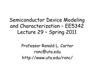
Join Professor Ronald L. Carter's lecture on semiconductor device modeling and characterization, presented on March 20, 2010. The session covers critical concepts such as the Onset of Strong Inversion (OSI), threshold voltage calculations for n-channel MOS capacitors, and key figures illustrating depletion and inversion states in silicon substrates. Upcoming class changes and project deadlines are announced. Explore the intricacies of n-channel and p-channel characteristics, as well as practical applications in semiconductor technology.

E N D
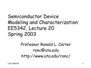
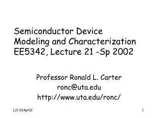
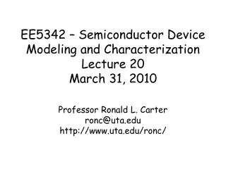
EE5342 – Semiconductor Device Modeling and CharacterizationLecture 20March 31, 2010 Professor Ronald L. Carter ronc@uta.edu http://www.uta.edu/ronc/
Schedule Change • Classes WILL be held on • 4/5/10 • 4/7/10 • Dr. Russell will be filling in • The previously scheduled make-up classes will be cancelled • 4/16/10 (Friday) • 4/23/10 (Friday) • Project 2 Test changed to W 4/28/10
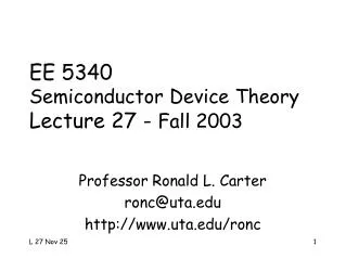
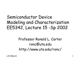
Inversion for p-SiVgate>VTh>VFB Vgate> VFB EOx,x> 0 e- e- e- e- e- Acceptors Depl Reg Vsub = 0
Inversion for p-SiVgate>VTh>VFB Fig 10.5*
Approximation concept“Onset of Strong Inv” • OSI = Onset of Strong Inversion occurs when ns = Na = ppo and VG= VTh • Assume ns = 0 for VG< VTh • Assume xdepl = xd,max for VG = VTh and it doesn’t increase for VG > VTh • Cd,min = eSi/xd,max for VG > VTh • Assume ns > 0 for VG > VTh
MOS Bands at OSIp-substr = n-channel Fig 10.9*
Equivalent circuitabove OSI • Depl depth given by the maximum depl = xd,max = [2eSi|2fp|/(qNa)]1/2 • Depl cap, C’d,min = eSi/xd,max • Oxide cap, C’Ox = eOx/xOx • Net C is the series comb C’Ox C’d,min
n-substr accumulation (p-channel) Fig 10.7a*
n-substrate depletion(p-channel) Fig 10.7b*
n-substrate inversion(p-channel) Fig 10.7*
fms (V) Fig 10.15* NB (cm-3) Typical fms values
Flat band with oxidecharge (approx. scale) Al SiO2 p-Si +<--Vox-->- q(Vox) Ec,Ox q(ffp-cox) Ex q(fm-cox) Eg,ox~8eV Ec EFm EFi EFp q(VFB) Ev VFB= VG-VB, when Si bands are flat Ev
Inversion for p-SiVgate>VTh>VFB Vgate> VFB EOx,x> 0 e- e- e- e- e- Acceptors Depl Reg Vsub = 0
Approximation concept“Onset of Strong Inv” • OSI = Onset of Strong Inversion occurs when ns = Na = ppo and VG= VTh • Assume ns = 0 for VG< VTh • Assume xdepl = xd,max for VG = VTh and it doesn’t increase for VG > VTh • Cd,min = eSi/xd,max for VG > VTh • Assume ns > 0 for VG > VTh
Fig 10.9* qfp 2q|fp| xd,max MOS Bands at OSIp-substr = n-channel
Computing the D.R. W and Q at O.S.I. Ex Emax x
n-channel VT forVC = VB = 0 Fig 10.20*
Fully biased n-MOScapacitor VG Channel if VG > VT VS VD EOx,x> 0 e- e- e- e- e- e- n+ n+ p-substrate Vsub=VB Depl Reg Acceptors y 0 L
Fully biased MOScapacitor in inversion VG>VT Channel VS=VC VD=VC EOx,x> 0 e- e- e- e- e- e- n+ n+ p-substrate Vsub=VB Depl Reg Acceptors y 0 L
Flat band with oxidecharge (approx. scale) Al SiO2 p-Si +<--Vox-->- q(Vox) Ec,Ox q(ffp-cox) Ex q(fm-cox) Eg,ox~8eV Ec EFm EFi EFp q(VFB) Ev VFB= VG-VB, when Si bands are flat Ev
MOS energy bands atSi surface for n-channel Fig 8.10**
Ex Emax x Computing the D.R. W and Q at O.S.I.
Q’d,max and xd,max forbiased MOS capacitor Fig 8.11** |Q’d,max|/q (cm-2) xd,max (microns)
n-channel VT forVC = VB = 0 Fig 10.20*
p-channel VT forVC = VB = 0 Fig 10.21*
Differential chargesfor low and high freq high freq. From Fig 10.27*
Ideal low-freqC-V relationship Fig 10.25*
Comparison of lowand high freq C-V Fig 10.28*
Effect of Q’ss onthe C-V relationship Fig 10.29*
n-channel enhancementMOSFET in ohmic region 0< VT< VG Channel VS = 0 0< VD< VDS,sat EOx,x> 0 e-e- e- e- e- n+ n+ Depl Reg p-substrate Acceptors VB < 0
Conductance ofinverted channel • Q’n = - C’Ox(VGC-VT) • n’s = C’Ox(VGC-VT)/q, (# inv elect/cm2) • The conductivity sn = (n’s/t) q mn • G = sn(Wt/L) = n’s q mn (W/L) = 1/R, so • I = V/R = dV/dR, dR = dL/(n’sqmnW)