Download
1 / 16
160 likes | 448 Vues
Workshop for NFF Nanoimprint System. NFF MA6 Nanoimprint Upgrade . Workshop for NFF Nanoimprint System. Outline. Nanoimprint Lithography (NIL) Upgrade Parts. Workshop for NFF Nanoimprint System. Nanoimprint Lithography (NIL).

E N D
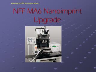
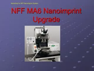
Workshop for NFF Nanoimprint System NFF MA6 Nanoimprint Upgrade
Workshop for NFF Nanoimprint System Outline • Nanoimprint Lithography (NIL) • Upgrade Parts
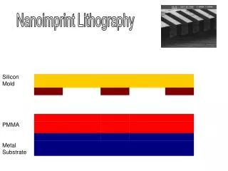
Workshop for NFF Nanoimprint System Nanoimprint Lithography (NIL) • Versatile, cost effective, flexible and high throughput (parallel) method for fabrication of down to 10 nm structures even over large areas (wafers) Applications in: •Semiconductormemory•Micro and nanofluidics •Optical devicese.g. LEDs and lasers •Life science, e.g. lab-on-a-chip systems, bio sensors•Radiofrequency components•Renewable energy•Security (holography, tags, etc.)•Nanotechnology
Stamp A stamp is fabricated by electron beamlithography (EBL) and dry etching Polymer Substrate The stamp is pressed into a soft thermoplastic, thermosetting or UV-curable polymer on a substrate combined with heating or UV radiation The polymer is cured and the stamp release from substrate Residual imprint polymer under stamp protrusion removed by‘descum’process Imprinted pattern transferred into substrate by dry etching Workshop for NFF Nanoimprint System Nanoimprint process
Workshop for NFF Nanoimprint System Upgrade Parts Include Stamp Stamp Holder Substrate Holder Stamping control
Workshop for NFF Nanoimprint System Stamp Bare Quartz Plate Patterned Stamp
Workshop for NFF Nanoimprint System Stamp Holder
Workshop for NFF Nanoimprint System Substrate Holder
Workshop for NFF Nanoimprint System Stamping ControlWith Firmware upgrade
Workshop for NFF Nanoimprint System Stamp Stamp Plate Dimension Stamp Pattern Anti- sticking Layer Stamp Handling
Workshop for NFF Nanoimprint System Stamp Plate Dimension Square Quartz Plate 65mm x 65mm x 6.35 mm thick A Square Shape Mesa ~ 25 um height at the center Probably 3 E-beam Alignment marks will be set nearly at the corners (will further discuss)
Workshop for NFF Nanoimprint System Stamp Pattern All pattern should be inside the Mesa area Standard Mesa size in NFF: 10 mm square Mesa can change to another size but it will take longer time to fabricate, more chance to jammed with the substrate and extra charge for new mesa mask Large patterned area also cause flatness problem of stamp To avoid drawing at boundary or a large enclosed pattern, especially near at the edges of Mesa. Because it will block the excess imprint resist flow
Unit cell S L dot Workshop for NFF Nanoimprint System • Beware of the imprint resist thickness to the depth of stamp pattern (Vtofill) of resist needed to fill completely this structure. For our design, Vtofill = Hm{LS + (L + S)S}, where Hm is the mould’s depth, L the dot’s size and S the spacing between each dot. Now the available volume of resist for this unit cell is Vresist = Hi (L + S)2, where Hi is the initial resist layer thickness. S Landis et al Nanotechnology 17 (2006) 2701–2709
Workshop for NFF Nanoimprint System Anti-sticking Layer • The Mesa is covered by an Anti-sticking layer • Anti-sticking layer is a very thin Fluorocarbon layer • Anti-sticking layer (>10 nm) for easy stamp release from a thin imprint resist • Don’t scratch the Anti-sticking layer • If Anti-sticking layer gets damage, it will cause jammed stamp during stamp releasing step or imprint resist stick onto the stamp surface
Workshop for NFF Nanoimprint System Stamp handling • Cleaning the stamp by Acetone, IPA, thinner and DI water ONLY. (No oxygen plasma, EKC or MS2001) • Before put the stamp back into the packing box, please make sure the box is dust free • Mesa side always face downward inside the packing box and don’t make it face upward even in normal case • Seal the packing box by adhesive tape if it will not be used for a period of time • Don’t touch the Mesa surface with anything else. • Of course, don’t drop it
Workshop for NFF Nanoimprint System Thank you for your attention!