Nanoimprint lithography (NIL)
Nanoimprint lithography (NIL). UV-curable NIL. Resists for UV-NIL. Mold fabrication for thermal and UV-NIL. ECE 730: Fabrication in the nanoscale : principles, technology and applications Instructor: Bo Cui, ECE, University of Waterloo; http://ece.uwaterloo.ca/~bcui/

Nanoimprint lithography (NIL)
E N D
Presentation Transcript
Nanoimprint lithography (NIL) UV-curable NIL. Resists for UV-NIL. Mold fabrication for thermal and UV-NIL. ECE 730: Fabrication in the nanoscale: principles, technology and applications Instructor: Bo Cui, ECE, University of Waterloo; http://ece.uwaterloo.ca/~bcui/ Textbook: Nanofabrication: principles, capabilities and limits, by Zheng Cui
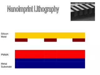
UV-NIL • Rome temperature, low pressure (1 - few atm). • Liquid resist consisting monomer, photo-initiator, coupling agent, surfactant… • Resist cross-link (become solid) upon UV illumination. • Mold (or substrate) needs to be transparent to UV. • Easy for alignment than thermal NIL, closer to optical lithography. • But resist side, thermal NIL resist is closer to optical lithography resist. For example, PMMA and SU-8 is both a photo-resist (PMMA for DUV lithography) and thermal NIL resist. • In fact, UV-NIL resist is closer to UV-curable glue. UV-NIL using dispensing resist UV light
Step and flash UV-NIL Resist is not applied by spin-coating; but drops by “inkjet”, less uniform thickness!! (for alignment) “Inkjet” system • Technology commercialized by Molecular Imprint Inc. • Resembles DUV stepper, die by die patterning (no need of a BIG expensive mold). • More favored by the semiconductor industry or wherever mold is too expensive.
Some examples of step and flash NIL In principle, UV-NIL has lower resolution than thermal NIL due to resist shrinkage (10%) upon cross-linking. In practice, UV-NIL has demonstrated similar resolution to thermal NIL.
UV-NIL using spin-on resist UV-resist Under-layer (PMMA, ARC…) • Typically bi-layer system, thin UV-resist layer to minimize shrinkage effects. • Resist contains Si, so can be used as a hard mask for etching under-layer with O2 plasma. • Spin-on resist is not suitable for step-and-flash NIL, because it must be imprinted quickly in one shot (liquid resist not as stable as thermal NIL resist in air, and it takes in dust quickly). • For R&D, spin-on resist is much more reliable than step-and-flash NIL, because the amplitude and uniformity of residual layer thickness is a big issue for drop-dispensed resist.
PDMS mold for UV-NIL • Transparent mold (also called stamp or template) in PDMS. • Flexible and soft for conformal contact to non-flat substrate. • But not for high resolution (<100nm), because PDMS is not hard enough and its nanostructure will deform under pressure. • One solution is using bi-layer, pattern in hard-PDMS or PMMA, which is spun on (regular soft) PDMS. • After oxygen plasma treatment, PDMS surface is like SiO2, so it is easy for silane anti-sticking treatment.
ZEP-520 mold (ZEP is an e-beam lithography resist) Because UV-NIL uses low pressure and room temperature, thermoplastic EBL resist such as PMMA and ZEP-520 can be used as a mold right after EBL and development. (may need anti-sticking surface treatment with silane, though not reliable on ZEP or PMMA.)
Dust • Dust is a bigger issue for UV-NIL than for thermal NIL because: • The liquid resist takes in dust easily from air, and the dust cannot be blown away. • The pressure is lower, leading to larger defect area with same size of dust particle. • So sometimes, UV-NIL is done at higher pressure to reduce defect area. UV-NIL dust particles
Critical dimension (CD) control in NIL CD control error budget comparison • Advantage of NIL for CD control: • No diffraction or proximity effects. • No lens aberrations. • Disadvantage of NIL for CD control: • 1 mask, so CD error on mask is printed onto resist without reduction. • Need a breakthrough etch of the residue layer, which adds CD error due to lateral etch. • But this error could be compensated in mask (mold) design.
Nanoimprint lithography (NIL) UV-curable NIL. Resists for UV-NIL. Mold fabrication for thermal and UV-NIL.
Resist for UV-NIL • UV-NIL resist has little in common with photo-resist, which resembles more thermal NIL resist. • In principle, any material that is soft (thus can be imprinted) and becomes hard upon UV exposure, can be used as UV-NIL resist. • For example, UV-glue for optical components and dental UV sealant, are UV-NIL resist. • Component of UV-NIL resist: • Organic acrylates provide low viscosity. • Organic cross-linker. • Additives: silicon-containing acrylate monomer, flourinated compounds. • Photoinitiator: cationic or free radical photoinitiator. • Photoinitiators: • Cationic photoinitiator: • Insensitive to oxygen, but low curing rates; and acids and heavy metals are harmful to semiconductors. • Free radical photoinitiator: • Great variety, high curing rates, but sensitive to oxygen, need vacuum or N2 environment curing.
UV curing at 375nm: curing time Typical curing time is a few seconds; oxygen is problem, need vacuum. Note: those resists are just examples, none of them are popular – in fact currently there is no single UV-resist that gains enough popularity – each company/researcher has its own small market share. Holger Schmitt, Christoph Lehrer
Adhesion mold/UV polymer/substrate Ideally: No adhesion between mold/UV-polymer. Strong adhesion between substrate/UV polymer. Interface reaction: Mechanical adhesion, wetting, specific adhesion that is mainly caused by inter-molecular bindings. is surface tension (N/m), also called surface energy (energy/m2=N/m) For substrate (Si, Si/HMDS, Si/ARC), low contact angle is better. For mold, high is better. Here, all resists still “wet” the mold (<90o)
Surface tension of various materials Contribution to total surface tension: polar and disperse part.
Adhesion of fluorinated UV resist to ARC coated substrates Summary of adhesion behavior: (green color is good)
Residual layer thickness For drop-dispensed resist (not spin coating) Thin (<<100nm) residual layer leads to less dimensional accuracy loss, so low viscosity (high flow rate) is desired. Conclusion: UV sealant and UV glue not appropriate. Certainly, residual layer thickness also depends on initial dispensed drop volume.
Summary for resist Curing chemistry: ideally it should be compatible with oxygen, so no need of vacuum. Curing speed: higher is better for faster imprint, typically few seconds curing time. Viscosity: lower is better, to fill large features faster, to have thinner residual layer. Surface energy: Since the resist has to “wet” the mold (contact angle <90 degree) for imprint using low pressure, both the mold and the resist have to have low surface energy for easy separation. Low surface energy resist may not adhere (wet) the Si substrate, making spin coating difficult or leading to resist peel off upon separation. One strategy is to coat an under-layer (PMMA, PMGI, ARC…) that binds well with the resist having low surface energy. If mold is coated with mold release agent (very low surface energy), the resist may still “wet” the mold if it also has low surface energy. (i.e. all the in the equation is small, one can still have <90o)
Nanoimprint lithography (NIL) UV-curable NIL. Resists for UV-NIL. Mold fabrication for thermal and UV-NIL.
Mold for thermal and UV-NIL Mold: also called template, stamp, master. Mold release agent: also called releasing layer, anti-sticking coating. Separation: also called de-molding, de-embossing, release. • Overview: • Usually fabricated from Si, quartz or nickel, though polymer mold is becoming more popular and available. • Feature fabrication at 1x vs. 4x for optical projection lithography, so critical dimension (CD) control at 1x more challenging. • For instance, photomask needs 250 nm resolution to print 65 nm features, NIL mold needs to be 65nm. • Desired properties: • Defect free fabrication & inspection, repairable. • Compatible to mold release agent coating. • Mechanically durable (for reuse). • Chemically durable (for cleaning). • Low CTE mismatch with substrate (coefficient of thermal expansion). • High imprint uniformity - uniform residual layer.
Comparison with photomask Optical projection lithography mask with OPC & equivalent NIL mold. OPC: optical proximity correction
Sidewall angle () < 90 = 90 > 90 Silicon PMMA Roughness (Ra) Polymer flow and filling property Align and imprint Resist deform Sticking Si De-mold Mold issues: profile, roughness, sticking
Mold release agent: Teflon-like coating Same idea as anti-stick cooking ware coating, but mono-layer. Silane by simple vacuum coating: clean wafer by oxygen plasma, put wafer and a drop of silane inside a container, and vacuum the container. After >5 hours, take wafer out and bake 150oC for 20min to cross-link the silane coating.
Ni mold • Si or SiO2 mold is most popular, but they are brittle. • Metal mold is more robust and durable, used for making CD/DVDs. • More difficult to fabricate, takes days for electroplating to 100s um. • Thickness is not uniform: much thicker (>2) plating near wafer edges. • Direct silane anti-stick coating to Ni not working, needs sputtering a thin (10nm) SiO2. • More used for hot-embossing onto thick plastics for micro/nano-fluidics applications. Source: Microelectron. Eng. 57-58 (2001) 375-380
SEM images of Ni molds Mold by electroplating (follows profile in resist, good) Mold by EBL and liftoff Easier to pattern metal by liftoff. But metal structure by lift-off doesn’t have vertical profile (-shaped), and is of low height. The underneath Si is still brittle. SEM image a of Ni/Si stamp showing 90nm channel-length inter-digited electrodes.
Soft PDMS/PMMA mold for UV-NIL PDMS PMMA Mold: PMMA top layer cast and bonded on a PDMS buffer and a glass carrier. Resist pattern: 0.1 atm imprint pressure, triangular lattices of 300nm period and 200nm pillar diameter. PDMS alone can be used as UV-NIL mold, but its nanostructure is not hard enough and will bend/collapse during NIL even at low pressure. It is good for m-feature size UV-NIL. Roy, “Enhanced UV imprint ability with a tri-layer stamp configuration”, MEE 2005
Soft PDMS/hard PDMS mold for UV-NIL Hard PDMS: more cross-linked PDMS, but more brittle and less flexible
Other polymer mold materials PTFE (Teflon, polytetrafluoroethylene), can be molded using a silicon mold at high temperature (>250oC). Low surface energy (no need for mold release agent), high strength, can do thermal NIL at high temperature. PVA (polyvinyl alcohol): water soluble, can be one-time use mold (imprint and dissolve the mold with water) ETFE (ethylene tetrafluoroethylene), similar to PTFE, but mold is easier to fabricate from a master mold. SSQ (silsesquioxane), similar to HSQ. After cross-linking the material is like SiO2, which is easy to coat with mold release agent. In principle, all cross-linked polymer can be used as NIL mold; however, most of them cannot be treated with mold release agent (hard to separate after imprint). Barbero, “High resolution nanoimprinting with a robust and reusable polymer mold” (ETFE), Advanced Functional Materials, 2419 (2007)
Diamond mold Diamond is hardest, but too expensive. Use diamond like carbon (DLC) film instead for mold. • DLC is a synthetic meta-stable form of carbon. • Amorphous network consisting of various fractions of hydrogen, SP2 and SP3 hybridized carbon. • Common synthesis techniques • Pulsed Laser Deposition • Ion beam deposition • Plasma Enhanced Chemical Vapor Deposition (PECVD) • And many other techniques • PECVD deposition uses hydrocarbon plasma in the presence of energetic ion bombardment. Ternary Phase Diagram1 • Why is DLC a suitable material for serving as the mold? • Excellent hardness and wear resistance 30-35 Gpa. • Low energy surface 35-50mN/m, may not need anti-stick coating. • Controllable band gap 1 to 3.5eV, for UV transparency. • High chemical and corrosion resistance. • Can be deposited on both Quartz and Si. • However, DLC deposition is very challenging, not readily available. J. Robertson, Materials Science and Engineering R 37 (2002), 129-281
Showerhead Electrode Precursor In Hydrocarbon Plasma Substrate Insulated rf feedthrough ~ DLC deposition by PECVD Energetic Ions, radical and atomic species created in the plasma are all critical Possible growth mechanism Typical PECVD reactor • DC and RF plasmas including microwave, capacitive and inductive-coupled plasmas. • Typical PECVD reactor • Reactor geometry, nature of RF coupling results in availability of energetic ions, radical and atomic species • Auxiliary electrode to control the ion-energies • Deposition mechanisms sub-plantation model, cylindrical spike model, …
Mold by MOCVD(?) and selective wet-etching Precise control of pitch and line-width. By far the highest resolution (6nm) NIL is demonstrated using such a mold. It is very difficult to write 14nm pitch grating using e-beam lithography.
Mold fabricated by nature Cicada Wings: a mold from Nature The cicada wings consist of ordered hexagonal close-packed arrays of pillars with a spacing of about 190nm. The height of the pillars is about 400nm and the diameters at the pillar top and bottom are about 80nm and 150nm, respectively.
Properties of cicada wings • Cicada wings have sufficientstiffness, chemical stability and low surface tension for NIL. • These properties originate from the arrangement of highly crystalline chitin nano-fibers embeddedin a matrix of protein,polyphenolsand water, with asmall amount of lipid. • Crystalline chitin interacts with theprotein matrix via hydrogen bonding, which gives stiffnessand chemical stability to the structure. • The Young’s modulus of these cicada wings can be as high as 7–9GPa. Although far lower than silicon (up to 131GPa), it is sufficient for imprinting PMMA while still maintaining the original profile. • There is a layer of wax on the surface of the wings, which contains esters, acids, alcohols, and hydrocarbons. This layer gives low surface tension, so no need of anti-stick coating.
Results of NIL using cicada wing mold Pressure 40 bar; temperature 190℃, 70℃ higher than the Tg of PMMA; imprint time 3min. The pitch between the wells is about 190nm, the well diameter is about 150nm, and the depth is found to be about 400nm; these are consistent with the mold.
Mold fabricated by engineer Mold fabricated by e-beam lithography and RIE. Gas Chemistry: Cr – Cl2/O2; SiO2 – CF4/O2 If no Cr RIE etch facility, Cr can be patterned readily by liftoff. Mold with TCO (transparent conducting oxide) • Incorporating TCO film in the mold has the following advantages: • Mold written by EBL without charge build-up. • Final molds are easily inspected (both CD and defects) with SEM. • It is still transparent for UV-NIL.
Etching issues for mold fabrication • Etch should be vertical or very near vertical. • But NO negative slope allowed • Trenching undesirable • Smooth sidewalls desirable • Uniform depth • Uniform critical dimension (CD) RIE trenching ICP etching offers better process control (ICP-inductively coupled plasma) Quartz ICP etching using Cr as mask • Cr mask etch followed by quartz etch. • 200nm depth for 30nm features (aspect ratio 7:1) • Etch rate 85nm/min. • Selectivity over Cr >170:1 (very high). • 89-90°profile (very vertical) • Smooth and trenching free.
ICP quartz mold etch: process control Control of trenching by DC bias Quartz etch using Cr mask Control of profile by temperature 100nm Cr etch using resist as mask Process gases: Cl2, O2 (+He). Cr etch rate >15nm/min. Uniformity <±4% (200mm wafer) Profile >85°. Delta CD<50nm. CD control < ±1%. Selectivity Cr : resist > 0.5 : 1 (resist dependent) resist quartz Cr
Pillar array mold fabrication white: Cr; purple: SiO2; blue: resist; black: silicon Pillar array (2D) mold fabricated from grating (1D) mold by two NILs