Download
1 / 19
220 likes | 843 Vues
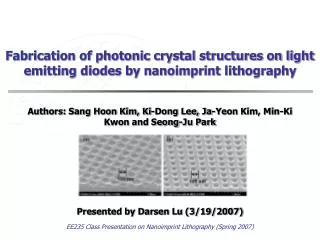
Fabrication of photonic crystal structures on light emitting diodes by nanoimprint lithography. Authors: Sang Hoon Kim, Ki-Dong Lee, Ja-Yeon Kim, Min-Ki Kwon and Seong-Ju Park Presented by Darsen Lu (3/19/2007). Outline. Introduction Some background Information Mold Fabrication

E N D
Fabrication of photonic crystal structures on light emitting diodes by nanoimprint lithography Authors: Sang Hoon Kim, Ki-Dong Lee, Ja-Yeon Kim, Min-Ki Kwon and Seong-Ju Park Presented by Darsen Lu (3/19/2007) EE235 Class Presentation on Nanoimprint Lithography (Spring 2007)
Outline • Introduction • Some background Information • Mold Fabrication • How to fabricate the mold for nanoimprint lithography • PCLED Device Fabrication • The fabrication of a photonic crystal light emitting diode (PCLED) using nanoimprint • Results • LED Performance Enhancement due to Photonic Crystal Structure EE235 Class Presentation on Nanoimprint Lithography (Spring 2007)
Introduction Some background Information EE235 Class Presentation on Nanoimprint Lithography (Spring 2007)
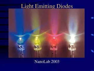
Light Emitting Diode (LED) • LED • Definition: a semiconductor device that emits incoherent narrow-spectrum light when electrically biased in the forward direction • LED v.s. Incandescent (Edison’s lightbulb) and Flourescent Bulbs • Much longer life span (105 - 106 hrs v.s. 103 / 104 hrs) • Suitable for applications that are subject to frequent on-off cycling • Efficiency: better than incandescent but currently worse than flourescent bulbs Source: US Department of Energy http://www.netl.doe.gov/ssl/faqs.htm Courtesy of Wikipedia http://en.wikipedia.org/wiki/LED EE235 Class Presentation on Nanoimprint Lithography (Spring 2007)
LED Efficiency • Internal Quantum Efficiency (ηint) • Definition: ratio of the number of electrons flowing in the external circuit to the number of photons produced within the device • Has been improved up to 80% • External Quantum Efficiency • Definition: The percentage of photons that can be extracted to the ambient. • Typically 1% ~ 10% • Limiting factor of LED efficiency • Improvement techniques: dome-shaped package, textured surface, photonic crystal, … Source: Lecture Note of “Optoelectronic Devices” (by Sheng-fu Horng, Dept. of Electrical Engrg, NTHU, Hsinchu, Taiwan) EE235 Class Presentation on Nanoimprint Lithography (Spring 2007)
Photonic Crystal • Photonic Crystal • Definition: Periodic optical nanostructures that are designed to affect the propagation of EM waves. • The periodic structure creates a “photonic bandgap.” No light with frequency within the gap can propagate. Source: SPIE Photonics West by Steven G. Johnson http://ab-initio.mit.edu/photons/tutorial/; EE235 Class Presentation on Nanoimprint Lithography (Spring 2007)
Photonic Crystal for enhancing the external quantum efficiency of an LED • Part of the extrinsic loss in LED • LED: a thin slab serves as a waveguide • At some frequencies, spontaneously emitted light can be coupled in to the waveguide Efficiency Loss • Photonic Crystal + LED • The “optical bandgap” prevents spontaneously emitted light from coupling into the waveguide, therefore enhancing the efficiency of the device. • PC Structure Design • Simulators are available: Ex: R-soft Source: Shanhui Fan, Pierre R. Villeneuve, and J. D. Joannopoulos, “High Extraction Efficiency of Spontaneous Emission from Slabs of PhotonicCrystals” EE235 Class Presentation on Nanoimprint Lithography (Spring 2007)
Mold Fabrication How to fabricate the mold for nanoimprint lithography EE235 Class Presentation on Nanoimprint Lithography (Spring 2007)
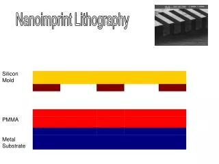
Mold Fabrication Process (1) • Start with a silicon wafer.Grow/Deposit layers: SiO2, Cr, Photoresist (PR) PR Cr SiO2 • Pattern the PR twice using a Laser Interference Lithography (LIL) • Develop the PR.Use a thermal treatment method to alter the pillar shape and increase its diameter EE235 Class Presentation on Nanoimprint Lithography (Spring 2007)
Mold Fabrication Process (2) PR • Use RIE to etch the Cr.Then use the Cr as a mask and etch SiO2 with RIE (This allows a thin PR layer) Cr SiO2 • Remove the Cr maskCoat Anti-sticking layer by vacuum evaporation EE235 Class Presentation on Nanoimprint Lithography (Spring 2007)
Thermal Treatment Method • Procedure: • Heat the wafer with PR at 120C for 5 minutes • Purpose: • Increase the pillar diameter (110nm to 150nm) • Control the shape of the photoresist pattern (circular) EE235 Class Presentation on Nanoimprint Lithography (Spring 2007)
Thermal Treatment Method (2) • 120°C is found to be the optimum temperature • Temperature too low no significant tampering effects • Temperature too high PR becomes too thin and lithography quality becomes poor EE235 Class Presentation on Nanoimprint Lithography (Spring 2007)
PCLED Device Fabrication The fabrication of a photonic crystal layer using nanoimprint EE235 Class Presentation on Nanoimprint Lithography (Spring 2007)
LED Device Fabrication • Remove the residual area using O2 plasma • Prepare an LED substrate sample. Deposit Cr and PR. • Nanoimprint Process (50bar, 145C) • Etch the Cr and p-GaN region EE235 Class Presentation on Nanoimprint Lithography (Spring 2007)
Results LED Performance Enhancement due to Photonic Crystal Structure EE235 Class Presentation on Nanoimprint Lithography (Spring 2007)
Device Performance Enhancement • LED intensity as a function of etch depth (With PC) With Photonic Crystal Structure: 9x Enhancement • LED intensity as a function of etch depth (Without PC) Control Group: 4x Enhancement (Due to “penetrating”) EE235 Class Presentation on Nanoimprint Lithography (Spring 2007)
SEM Pictures • (a) FESEM Image of the LED sample after removal of the residual layer and Cr Patterning • (b) Final PC strctures on a p-GaN layer • The diameter of the hole increases after each patterning FESEM: Field Emission Scanning Electron Microscope EE235 Class Presentation on Nanoimprint Lithography (Spring 2007)
Summary • The energy efficiency of an LED can be improved by enhancing the external quantum efficiency. • Photonic Crystal is one of the possible mechanisms to enhance the external quantum efficiency • A mold is fabricated using laser interference lithography (LIL) and thermal treatment method • A Photonic Crystal LED is fabricated using nanoimprint lithography • The light intensity of the LED is significantly improved due to the photonic crystal structure EE235 Class Presentation on Nanoimprint Lithography (Spring 2007)
The End • Thank you • Questions? EE235 Class Presentation on Nanoimprint Lithography (Spring 2007)