Exploration of Nanoscale Noise in Metal Surfaces: Insights from University of Maryland's Research
At the University of Maryland, researchers have delved into the nanoscale noise phenomena within electronic devices, revealing crucial insights through time-resolved Scanning Tunneling Microscopy (STM) imaging. Their studies show that motion of surface line boundaries (steps) correlates significantly with electrical carrier scattering, resulting in noise signatures that diverge from traditional predictions. This groundbreaking work enhances our understanding of surface resistivity variations due to step fluctuations, with implications for the design of nanoscale electronic components.

Exploration of Nanoscale Noise in Metal Surfaces: Insights from University of Maryland's Research
E N D
Presentation Transcript
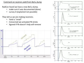
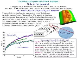
Current uphill Current downhill University of Maryland NSF-MRSEC Highlight: Noise at the Nanoscale Chenggang Tao, A. Bondarchuk, W.G. Cullen P. Rous, T. Bole and E.D. Williams Phys. Rev. Lett. 99, 206801 (2007); New J. Physics 9, 387 (2007); Surface Sci. 601,4939 (2007) Ellen D. Williams, University of Maryland College Park, DMR 0520471 In nanoscale devices, we have the opportunity to isolate the individual physical processes of noise. Time-resolved STM imaging of fluctuating nanoscale structure shows that the motion of surface line boundaries (steps) is coupled 10x more strongly to scattering of electrical carriers than predicted from zero-temperature calculations. The resulting changes in surface resistivity will carry the spectral characteristic of the step fluctuations, yielding a distinct noise signature SI ~ f-3/4. Scattering at Nanoscale Structure in Metals Top above: Scanning Tunneling Microscope (STM) image of the top of a 20 nm diameter crystalline Ag wire. The longitudinal structures are steps - changes in height by a single atomic layer. Middle above: Schematic illustration of the scattering of charge carriers at surface steps, with expanded image illustrating the thermal excitations of the atomic structure that cause step motion. Bottom Left: The thermal motion of the steps, shown by the correlation function G(t), is enhanced or suppressed when current flows uphill or downhill with respect to the step direction