Download
1 / 18
180 likes | 211 Vues
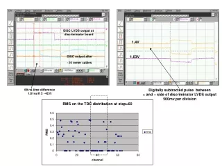
DISC LVDS output at discriminator board. 1.4V. DISC output after ~10 meter cables. 1.63V. 69 ns time difference 1.61ns/ft ~42 ft. Digitally subtracted pulse between + and – side of discriminator LVDS output 500mv per division. Test pulse setting 0x60 ~ 4mv input 8 mv per step.

E N D
DISC LVDS output at discriminator board 1.4V DISC output after ~10 meter cables 1.63V 69 ns time difference 1.61ns/ft ~42 ft Digitally subtracted pulse between + and – side of discriminator LVDS output 500mv per division
Test pulse setting 0x60 ~ 4mv input 8 mv per step. CMS Disc threshold Channel 26 Channel 26 Channel 28 TDC Channel 30 Channel 32 Channel 32 Threshold (8 mv per step) TDC distribution at step =20 (160mv)
Test pulse setting 0x40 ~ 2.7 mv input 8 mv per step.
Test pulse setting 0xc0 ~ 8mv input 8 mv per step. Channel 26 Channel 26 Channel 32 Channel 32
Test pulse input 4 mv per step.
Test pulse input 4 mv per step. New chip, DC/AC ground jumper connected Channel 14 TDC distribution, DAC step =80 Chnl=14
Test pulse setting 0x60 ~ 4mv input 8 mv per step. New chip ground tight Channel 26 Channel 26 Channel 28 Channel 32
Test pulse setting 0x60 ~ 4mv input 8 mv per step. New chip ground disconnected.
Test pulse input 4 mv per step. New chip, Analog/digital ground separated. Channel 14 TDC distribution, DAC step =80
Pulse injection into chnl =47 At step 60, pulse height is equal to 30mv Chnl=48 Chnl=47 Chnl=46
Pulse injection into chnl =47 At step 60, pulse height is equal to 120mv
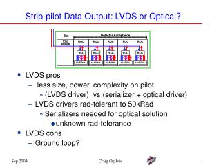
For RPC1, RPC3 N will be 12 data from 6 FEM with current design. For RPC 2 N will be 8 data from 4 FEM with current design Maximum we can be 10 cable inputs per connector We will have 2 optical transceivers per board Optical bandwidth will be 20bits * 140 MHz 16 bits data word into TLK Carrier extend Data word N Data word 1 Header Upper byte of the status word could be module ID + error bits Lower byte could beam clock counter
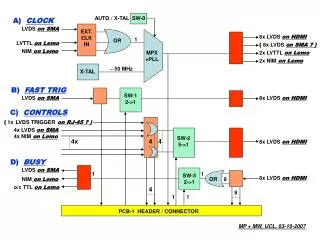
L1 primitives XMIT T D C T D C Output To L1 Clock fanout Clock Master TDCs Slow Control GTM DCM L1 RPC(HBD) crate/BUS structure 6Ux160 mm VME size
RPC TDC MODULE Interface Chip Collects 64 Channel Of Data L1 trigger primitives TDC serial download Trigger window L1 trigger primitives Event Data 32 channel digitizer D I S C Disc Serial download LVDS Transmitter MASK Digitized Data LVDS Receiver Serial Download Timing etc. L1 trigger etc Event Data 44X BC Test Pulse Serial download PLL Test Pulse 44X BC 4x beam clock
Channel count etc… (one side) The crate size is like 6U VME crate. I would like to limit the length discriminator cable to 10 meters. (to be tested about jitters) The RPC2, 3, we will need to find the crate space near the detector. Crate need to be recess in the rack. Cable routing space needed in front of the crate.
Channel count etc with RPC2/3 strips combined… (one side) The crate size is like 6U VME crate. I would like to limit the length discriminator cable to 10 meters. (to be tested about jitters) The RPC2, 3, we will need to find the crate space near the detector. Crate need to be recess in the rack. Cable routing space needed in front of the crate.