COMP541 Sequential Circuits
COMP541 Sequential Circuits. Montek Singh Feb 1, 2012. Topics. Sequential Circuits Latches Flip Flops Verilog for sequential design Example: A simple counter. Sequential Circuits. State of system is info stored That, and inputs, determine outputs. Types of Sequential Circuits.

COMP541 Sequential Circuits
E N D
Presentation Transcript
COMP541Sequential Circuits Montek Singh Feb 1, 2012
Topics • Sequential Circuits • Latches • Flip Flops • Verilog for sequential design • Example: A simple counter
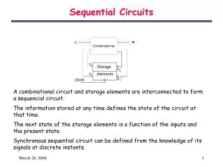
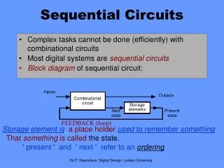
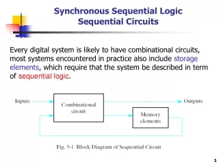
Sequential Circuits • State of system is info stored • That, and inputs, determine outputs
Types of Sequential Circuits • Synchronous • State changes synchronized by one or more clocks • Asynchronous • Timing of changes are independent of any clocks
Clocking of Synchronous • Changes enabled by clock
Comparison • Synchronous • Easier to analyze because can factor out gate delays • Set clock so changes occur before next clock pulse • Asynchronous • Potentially faster • Harder to analyze (more subtle, but more powerful!) • Most of my research! • Will look mostly at synchronous
Storage Elements • Latch • Flip-Flop – a latch that transitions on a clock • Registers • Addressable memories or banks of registers
Basic Storage • Apply low or high for longer than tpd • Feedback will hold value
Bistable Circuit Analysis • Consider 2 possible cases: • Q = 0: then Q’ = 1 and Q = 0 (consistent) • Q = 1: then Q’ = 0 and Q = 1 (consistent) • Bistable circuit stores 1 bit of state in the state variable, Q (or Q’) • But there are no inputs to control the state
SR (set-reset) Latches • Basic storage made from gates • S & R both 0 in “resting” state • Have to keep both from 1 at same time
Latch • Similar – made from NANDs
SR Latch Summary • SR stands for Set/Reset Latch • Stores one bit of state (Q) • Control what value is being stored with S, R inputs • Set: Make the output 1 (S = 1, R = 0, Q = 1) • Reset: Make the output 0 (S = 0, R = 1, Q = 0) • Behavior undefined/invalid when: • S = R = 1
Add Control Input • Gates when state can change • Is there latch w/ no illegal state?
D-type Latch • No illegal state
Transparency of latches • As long as C (the control )ishigh, state can change • This is called transparency • What’s problem with that?
Effects of Transparency • Output of latch may feed back • May cause/allow further state changes • Behavior depends on actual gate delays • Want to change latch state only once • Behavior should depend only on logical values
Solution to Transparency: Flip-Flops • Flip-Flops: • Ensure output changes only once per clock cycle • Two commonly-used types of flip-flops: • Master-Slave • Use a sequence of two latches • Edge-Triggered • Implementation very different from latches
1. Master-Slave Flip-Flop • Either Master or Slave is enabled, not both
Timing Diagram • Trace the behavior • Note illegal state • Is it transparent?
Have We Fixed the Problem? • Output no longer transparent • Combinational circuit can use last values • New inputs appear at latches • Not sent to output until clock low • But changes at input of FF when clock high do trigger next state • Is this a problem? • As clock faster, more problems • Have to guarantee circuit settles while clock low
2. Edge-Triggered Flip-Flops • New state latched on clock transition • Low-to-high or high-to-low • +ve edge-triggered, -ve edge-triggered • Also: dual-edge-triggered • Changes when clock high are ignored • Note: Master-Slave sometimes called pulse triggered
D-Type Edge-Triggered • Is this +ve or –ve edge-triggered?
Standard Symbols – Latches • Circle at input indicates negation
Symbols – Master-Slave • Inverted ‘L’ indicates postponed output • Circle indicates whether enable is positive or negative • JK: like an SR flip-flop, but: • If J=K=1, output is toggled • Can make a toggle flip-flop (T flip-flop) from a JK
Symbols – Edge-Triggered • Arrow indicates edge trigger
Direct Inputs • Use to force Set/Reset independent of clock • Direct set or preset • Direct reset or clear • Often used for power-up reset
Counters • Increments on each clock edge • Used to cycle through numbers For example, • 000, 001, 010, 011, 100, 101, 110, 111, 000, 001… • Not necessarily binary • Example uses: • Digital clock displays • Program counter
Verilog for Sequential • New Verilog to describe sequential circuits • Can use latches and flip-flops from library in schematic capture or Verilog • And connect them using wires • But more productive to write higher-level Verilog description
Register Data Type • Like wire but value is retained over time • Often causes latch or FF to be synthesized • Examples reg state; reg [15:0] addr;
Always Block • Example always @ ( sensitivity list ) statement; • Sensitivity list determines what might affect statements • Could think of it as “statement is run when one of values in sensitivity list changes value” • Example next
Synthesize a Flip-Flop module flop (C, D, Q); input C, D; output Q; reg Q; always @(posedge C) begin Q = D; end endmodule negedge also possible
Blocking Assignment • Equal sign indicates blocking statements initial begin B = A; C = B; end • Result is that new contents of B are in C, so all have contents of A.
Non-Blocking Assignment • <= indicates non-blocking statements initial begin B <= A; C <= B; end • All RHS evaluated first, then assigned • Result is that old contents of B are in C • This is what is normally synthesized!!!
This is Not Software! • Don’t assign to same reg in more than one always block • The always blocks are concurrent • Doesn’t make sense to set reg from two signals • Assignments in always blocks should be non-blocking • You usually don’t mean sequential execution • Can’t synthesize anyway!
Asynchronous Reset module dff_v(CLK, RESET, D, Q); input CLK, RESET, D; output Q; reg Q; always @(posedge CLK or posedge RESET) begin if (RESET) Q <= 0; else Q <= D; end endmodule
Synchronous Reset always @(posedge CLK) begin if (RESET) state <= 0; else state <= D; end
Verilog for a Counter module counter(input clk, output [23:0] cnt ); reg [23:0] cnt; always @ (posedge clk) cnt <= cnt + 1; endmodule
Simulation vs Synthesis • If you don’t initialize regs in your circuits, simulator will complain • many values will be X • Electronics will work OK • each reg in actual circuit will “wake up” to a 0 or 1 value
Verilog 2001 Syntax • Can initialize regs at declaration reg onebit = 1’b0; reg [3:0] fourbits = 4’b1011; reg [23:0] cnt = 0;
Topics • Today • Looked at basic latches • Flip-flops • Verilog for sequential circuits • Simple counter
Read • Textbook Ch. 3.1-3.3 for today • Ch. 3.4-3.5 for next class
Next Time • State Machines • Verilog to describe state machines

