Time projection chambers
This document discusses the design and operational principles of Time Projection Chambers (TPC) and Micro-Pattern Gas Detectors (MPGDs) for high-energy physics applications. Emphasis is placed on reducing transverse diffusion, enhancing spatial resolution, and achieving large amplification gains through novel techniques like Gas Electron Multipliers (GEMs) and Micromegas. The challenges of utilizing gases, handling ion buildup, and ensuring low contamination levels are addressed, alongside the operational dynamics of silicon detectors. These advancements pave the way for efficient particle detection systems suitable for collider experiments.

Time projection chambers
E N D
Presentation Transcript
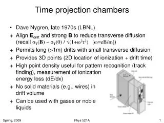
Time projection chambers • Dave Nygren, late 1970s (LBNL) • Align Edrift and strong B to reduce transverse diffusion (recall σT(B) ~ σT(0) / √(1+ω2τ2) [ω=eB/m]) • Permits long (>1m) drifts with small transverse diffusion • Provides 3D points (2D location of ionization + drift time) • High point density useful for pattern recognition (track finding), measurement of ionization energy loss (dE/dx) • No solid materials (e.g., wires) in drift volume • Can be used with gases or noble liquids Phys 521A
TPC operation • Choose gas with intrinsically small diffusion; centroid position resolution is σD / √nT • Long drift distance sensitivity to attachment, E distortions • Careful design/fabrication needed • O2 contamination <10-4 to reduce attachment • Ion buildup can distort field (gating grid needed) • Long drift time (up to 0.1 ms) need to correlate ionization with “zero time” for particle • bunch crossing times in colliders can be 100ns or less • Not an issue in other environments Phys 521A
Gas amplification issues • Require large (>10 kV/cm) E field for amplification, so high voltage must be supplied to device • In TPC, 2D position coordinate is based on charge induced on segmented readout pads • Gas amplification still occurs near thin anode wires above pads; radial E field there causes unwanted ExB effects, worsens resolution • Feature size (many mm) of wire-based amplification large compared to desired resolution (< 0.1mm) • Situation greatly improved by new technology for gas amplification: MicroPattern Gas Detectors Phys 521A
Micro-Pattern Gas Detectors - GEM • Gas Electron Multipliers (GEMs), introduced by Sauli. • Consist of insulating foils with conductive surfaces with regular pattern of small-diameter etched holes • Hole pitch typically ~200μm, hole diameter ~50μm, sheet thickness h ~ 50μm • Modest voltage difference leads to fieldE ~ V / h ~ (200V / 5*10-3cm) = 40kV/cm in holes, providing amplification • Several GEMs in series can provide amplification of 104 or more • Readout electrodes can operate at unit gain, reducing restrictions on geometry Phys 521A
Micro-Pattern Gas Detectors - Micromegas • Micromesh gaseous structure (Micromegas) introduced by Giomataris • Small amplification gap; variations in gap size lead to competing effects on E, 1st Townsend coefficient α • Fine anode pattern provides good spatial resolution • Operating voltage ~40 kV/cm * 0.01cm~ 400V between anodeand HV2 • Integrated manufacturingtechnique possible (in usefor T2K TPC) Phys 521A
Large area gas detectors • Need to instrument large areas (e.g. 100’s of m2 for muon detectors) places cost constraints; need cheap and reliable technology • Still desire good (sub-mm) position resolution • Calls for simple detectors operating in limited streamer mode to produce large signals, since electronics needs to be cheap too (Geiger mode results in long recovery times) Phys 521A
RPC – resistive plate chambers • Consist of few mm gap between highly resistive and flat planes of glass or ceramic with a high potential (~10kV) across them • Discharge from passing particle quenched as local field drops below amplification field • Localization based on capacitively-coupled strips on outer surfaces Phys 521A
Solid state tracking detectors • Semiconductors (typically silicon) can be used to detect charged particles; electron-hole pairs are created with threshold of few eV • Low threshold relative to ionization results in much larger production of e-h pairs per gm/cm2, allowing detectors to be thin (typically ~250μm) • Devices resemble photodiodes but with segmented electrodes on one or both surfaces • Fine segmentation (strip or pixel separation ~25-100μm) allows spatial resolution as small as 10μm • Response to deposited energy is also sensitive and linear, allowing use as active medium in calorimeters Phys 521A
Basic operation of silicon sensors • Operated with modest reverse bias to facilitate charge collection (but without amplification) • Resultant signals are small, so small capacitance is desirable (typically ~1 pF/cm of strip length) • Electron and hole mobilities (drift speed / field) differ: • Electrons have μ ~ 1350 cm2 V-1s-1 • Holes have μ ~ 450 cm2 V-1s-1 • Typical charge collection time in 300μm ~ 30 ns • Energy needed for e-h pair is 3.67 eV (at room temp) • Most probable # e-h pairs in 300μm wafer is 22,000 • Fano factor F~0.1 [recall σN/N = √(F/N)] Phys 521A
Types of detectors • Single-sided strips (readout on p-side) • Double-sided strips (requires n-side readout as well) • Pixels (bump-bonded to readout) • Detector parameters • Thickness (signal/noise [aim for ~15] vs. multiple Coulomb scattering) • Strip pitch (resolution vs. capacitance, # of channels) • Pixels (resolution vs. # of channels) • Detectors cut from single-crystal ingots; ingot diameter of 3 – 6 inches limits maximum sensor size Yield is smaller for larger-area chips Phys 521A
ATLAS pixel module (one of 1744) Phys 521A
Moore’s law for silicon detectors • There has been exponential growth in the area instrumented with silicon detectors and a concomitant rise in the number of readout channels • This is possible due to the reliance on similar fabrication techniques to those used in large-scale chip making; the cost per m2 of silicon detectors has dropped rapidly Phys 521A
Radiation damage • Extensively studied due to the use of silicon sensors in “vertex detectors” located just outside the accelerator beam pipe, where particle fluxes are highest • Sensitive to defects present in silicon crystal • Trapped charge affects electrical characteristics; changing bias voltage can compensate to a point • In general, detectors have degraded signal/noise with increasing dose • Damage also strongly dependent on temperature; large gain if sensors are always kept cold (damage occurs even with beam off if they warm up) Phys 521A
BaBar vertex detector CMS endcap tracker Silicon bonding and detector pics http://hep.ph.liv.ac.uk/~tara/lhcb_outreach/animations.html Phys 521A
Diamond sensors • Lightest semiconductor • Some differences with respect to Silicon: • Large band gap (5.5 eV, vs 1.1 for Si) • Lower signal (few thousand e-h in 300 μm) • Saturation velocity ~ 2.5x Si fast charge collection • e-h pairs/mip/μm ~36 (90 for Si) • Radiation hard (x10 or better) • Low capacitance, leakage current • Used in high radiation environments (beam monitors, radiation sensors • Diamond is a bit harder to grow than Si… use poly-crystalline CVD (chemical vapor deposition) material Phys 521A