Download
1 / 20
200 likes | 372 Vues
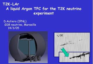
The Back-End Electronics of the Time Projection Chambers in the T2K Experiment. D. Calvet 1 , I. Mandjavidze 1 , B. Andrieu 2 , O. Le Dortz 2 , D. Terront 2 , A. Vallereau 2 , C. Gutjahr 3 , K. Mizouchi 3 , C. Ohlmann 3 , F. Sanchez 4 1 CEA/DSM/IRFU/SEDI, Saclay, France

E N D
The Back-End Electronics of the Time Projection Chambers in the T2K Experiment D. Calvet1, I. Mandjavidze1, B. Andrieu2, O. Le Dortz2, D. Terront2, A. Vallereau2, C. Gutjahr3, K. Mizouchi3, C. Ohlmann3, F. Sanchez4 1CEA/DSM/IRFU/SEDI, Saclay, France 2CNRS/IN2P3/LPNHE, Paris, France, 3TRIUMF, Vancouver, Canada 4IFAE, Barcelona, Spain
Tokai to Kamioka (T2K) experiment 50 kT water • Main Physics Goal: neutrino oscillation • nμ disappearance for improved accuracy on q23 • ne appearance to improve sensitivity to q13 Experiment now taking data 2
T2K Time-Projection Chambers 1 m 2 m 1 of 3 TPCs shown • Summary of features • Amplification: MicroMegas modules segmented in 7 x 10 mm pads • Over 124.000 pads to instrument ~9 m2 sensitive area 3
T2K TPC-FGD readout: AFTER chip 16 values 4 Rf*Cf (100us) Rf Cf Cp x511 Cs in Cs Memory Cell VdcinG-2 + - CSA Rp ADC in - + Cl Cm Vdc 16 values 2*Cg2 Cdet Cg2 pole zero cancellation Cg Gain-2 Sallen&Key Filter ckw ckr r2 r1 + - vicm r1 Buffer r2 Cs + - 2*Cg P. Baron et al. • 72 Analog Channels • Switched Capacitor Array: 511 cells • 4 Gains; 16 Peaking Time values (100ns to 2µs) • Input Current Polarity: positive or negative • Readout: 76*511 cells at 20MHz [external 12bits ADC] ADCin 2V/10MIPs Tp(5%-100%) ns 116 610 1054 1546 200 695 1134 1626 412 912 1343 1834 505 993 1421 1912 ckw: 1MHz-50MHz ckr: 20MHz Noise < 2mV denis.calvet@cea.fr 4
TPC Read-Out Diagram 124.414 detector pads 72 Front-End Electronic Modules On-detector in magnet Clock/Trigger 72 x 2 Gbps fibres ~20 m Control/Data 18 Quad-opticallink Data ConcentratorCards Off-detector back-end electronics Slave Clock Module 18 24-ports Gbit Ethernet Switch Master Clock Module On-line database Global event builder Run control Mass storage Nd 280 network TPC DAQ PC • Back-end elements • Data Concentrator Cards (DCCs) to aggregate data from front-end • Gbit Ethernet private network and PC for TPC local event building 5
Data Concentrator Cards • Main requirements • Fanout global 100 MHz clock, synchronous trigger to front-end with low skew (< 40 ns) • Aggregate data from multiple front-ends (typ. 4 modules per DCC, i.e. 7000 channels). Target DAQ rate: 20 Hz • Configure front-end and read-back run-time settings • Interfaces • to TPC DAQ PC through standard Gbit Ethernet switch • to front-end via 72 duplex optical links – 2 x 144 Gbps aggregate • to Slave Clock Module via dedicated LVDS links • Design strategy • Development of dedicated board too slow to meet project deadlines • → Extend platform used for single module readout; scale it up to full size system by trivial duplication • → Common hardware design with T2K Fine-Grain Detector (FGD) toshare development effort 6
Doing more with an evaluation board 3+1 optical ports Gbit Ethernet 100 MHz ref. Clock Trigger input RJ45 PLL 7
DCC Close-up 1 of 18 DCCs Xilinx ML405 Evaluation Platform Optical link extension card Clock board External Clock Trigger input • Design risks and benefits • Optical link board easily adds 3 SFP transceivers to ML405 • External clock distribution requires hardware modification of ML405 • → Lowest cost, minimal design effort and shortest deployment time solution 8
DCC Transmitters Eye Diagram On-board SFP Link via SMA Link via SATA#2 Link via SATA#1 Prototype: Local 25 MHz local oscillator + LMK03000 PLL multiplication for 200 MHz RocketIO reference Final design: Silicon Laboratories Si5326 PLL denis.calvet@cea.fr 9
DCC Optical Transmitter Jitter Optical link on SATA#2 connector • Remarks • Clock quality not significantly degraded by add-on cards and modifications on ML405 board • In real experiment 100 MHz ref. clock have to use cat. 6 cable (~1 m) • → All 72 links in final system running stably – Estimated BER < 10-15 denis.calvet@cea.fr 10
Clock/Trigger fanout capability DCC Clock FEM#1 Clock FEM#2 Clock Recovered clock on 2 FEMs compared to DCC reference clock (16 ns primary reference clock) DCC to FEM path delay variations over 100 FPGA reconfigurations (16 ns primary reference clock) • Remarks • Phase of recovered clock on Virtex 2 Pro / 4 RocketIO w.r.t. phase of sender not predictable from one system configuration to the next – but remains stable (<~2 ns) after link synchronized • Limited control of skew of synchronization signals sufficient for this TPC • → R&D on Virtex 5: predictable latency achievable with GTP transceivers denis.calvet@cea.fr 11
TPC Backend Electronics Crate 1 of 3 DCC crates • Principles • Each DCC mounted on an aluminum plate • 6 DCCs per 6U crate (i.e. 1 crate reads-out 1 TPC or 1 FGD) • All cables and fibers at the back; CompactFlash (firmware) at the front • → Most practical way found to rack-mount non-standard form factor cards 12
Complete TPC Back-end System Front-end Power & Slow Control Rack Back-end Electronics Rack Front-end slow control PC Slave clock module Ethernet switch Power supply Front-end power supplies (2 Wiener PL508) Crates of DCCs Power supplies 13
DCC Embedded Firmware/Software to/from front-end via optical links to/from TPC DAQ PC PowerPC 405 (300 MHz) rx RocketIO 1K-32bit PHY Ethernet MAC tx rx RocketIO 1K-32bit tx Cache controller DMA rx RocketIO 1K-32bit Multi-port Memory controller tx 128 MB DRAM D-Cache I-Cache rx RocketIO 1K-32bit tx • Principles • Use hard IP blocks of Virtex 4: transceivers, processor, Ethernet MAC… • Finite state machine in user logic pulls data from 4 front-ends in parallel • Standalone server program in PowerPC 405 unloads front-end data, elementary checks, uncapsulates in UDP/IP frames sent by MAC Processor Local Bus 32/64-bit 100 MHz User Logic Data-Side-On Chip Memory bus 32-bit 100 MHz Virtex 4 FPGA 14
Hard-wired data collection FSM SendEnable<3..0> PowerPC 405 (300 MHz) Sender 0 To RocketIO TX Sender 1 1896 entry LUT ZS 1111 ZS 0000 Sender 2 PLB 32-bit 100 MHz ZS 0011 Sender 3 Next Channel F (0 to 5) A (0 to 3) C (0 to 78) counters request ZS, FEC, ASIC, Channel Start event Rx FIFO 0 Free > 2 KB Finite State Machine FromRocketIO RX Fifo’s & Rx FIFO 1 Free > 2 KB Suspend Abort Rx FIFO 2 Free > 2 KB Rx FIFO 3 Free > 2 KB • Operation • Requests data channel by channel from 4 front-end modules in parallel • Suspends if any FIFO cannot store data of next request • Next request posted automatically when data of pending request entirely received or pre-defined timeout has elapsed 15
T2K Nd280 DAQ system fetpcdcc 0 TPC DAQ PC Local event builder to/from DCCs via private Gbit Ethernet switch Cascade … See: R. Poutissou et al., “Cascading MIDAS DAQ Systems and Using MySQL Database for Storing History Information”, this conference fetpcdcc 17 FGD DAQ PC Global DAQ PC nd280 network PODDAQ PC Global event builder xxx DAQ PC See: M. Thorpe et al., “The T2K near Detector Data Acquisition Systems”, this conference • Architecture • Local event building in TPC DAQ PC • Bridge to MIDAS global event builder via Cascade • Private nd280 network provides access to services shared by other detectors in the experiment On-line database, Mass storage, etc. 16
TPC DAQ System Performance T2K laser events T2K beam, cosmic events Event acquisition time for 1 DCC in full readout mode Event acquisition rate for 1 front-end module in zero-suppressed mode • Global system performance in running conditions of T2K • 33 Hz event taking rate in zero-suppressed mode (required: 20 Hz) • 50 ms latency for laser calibration events (1 DCC in full readout mode) • Max. DCC throughput: 16 MB/s (limitation: PPC405 I/O over DS-OCM) • Global throughput linear with # of DCCs until GbE link saturation • → All requirements met – system in exploitation 17
Experience Return Beam spill + Cosmic events Mean: 3.5 kB A cosmic event seen at T2K Nd280 Typical TPC event size: ~65 kB (spill or cosmic) 750 kB on 1 DCC for laser calibration events • System robustness and stability • All optical links very stable despite sub-optimal clocking; BER < 10-15 • Clock skew stable in operation but variation from one power-up to next • No hardware failure after ~6 months of operation • Need improve handling of oversized events to minimize deadtime • → Successful assembly of production system from evaluation hardware 18
Summary • Purpose of the development • A 1-to-72 clock-trigger fanout tree plus a 72-to-1 data aggregation system. Bridges TPC front-end 144 Gbps optical path to 1 Gbit Ethernet on DAQ side • Key elements • 18 Xilinx Virtex 4 evaluation boards with minimal add-ons + off-the-shelf PC and Ethernet networking products • Performance and limitations • Clock distribution stable during operation but each link settle to a different skew (~40 ns p.p.) at system power-up due to Virtex 2Pro / 4 RocketIO limitations – other R&D show this can be much better controlled with Virtex 5 • Limited I/O capability of PPC405, DOCM faster than PLB. Our application: 130 Mbit/s usage of Gbe link – by-pass processor if one needs to fully exploit Gbe • System pros and cons • Low-cost and shortest deployment time solution. Evaluation kits not meant for production systems…but it works! See poster: Y. Moudden et al., “The level 2 trigger of the H.E.S.S 28 meterCerenkovtelescope” 19
Outlook • FPGA board design is getting more and more complex • Manufacturer has to provide many guidelines, notes, reference design schematics…but still need skilled designers / layout engineers to build your own board. Time consuming, technical risks at design and production • Many applications require same common blocks beyond FPGA itself • De-coupling capacitors, external memory (DDR2, 3), configuration Flash, several high speed serial links, many customizable user I/O, flexible clocking • Evaluation boards • Originally to help designers make their own board design. Brings very latest FPGA technology instantly to anyone at low cost and no risk. An eval board has a lot in common with the core of a typical end product – why re-invent? • Think evaluation boards (have them made) as macro-components? • Worked for us. Improvements: lower-profile (2 cm stacking), smaller form factor, access to more user I/O and high speed serial links, flexible clocking • → Towards a better eval. board paradigm?: FPGA + SDRAM + Flash, I/O connectors on a general purpose module directly re-usable by customer; the element for demo is the carrier board (largest diversity of interface standards) denis.calvet@cea.fr 20