A Multiple Clock Cycle Instruction Implementation
A Multiple Clock Cycle Instruction Implementation. Comments on Single-Cycle Implementation. Machine instructions may have different critical path length Load instruction FP instructions Different addressing mode The cycle time will be detremined by the worst critical path

A Multiple Clock Cycle Instruction Implementation
E N D
Presentation Transcript
A Multiple Clock Cycle Instruction Implementation \course\cpeg323-05F\Topic5b-323.ppt
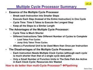
Comments on Single-Cycle Implementation • Machine instructions may have different critical path length • Load instruction • FP instructions • Different addressing mode • The cycle time will be detremined by the worst critical path • FU duplication may be costly \course\cpeg323-05F\Topic5b-323.ppt
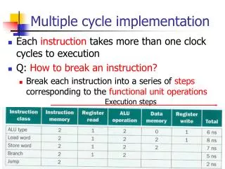
Multi-Cycle Implementation • Each instruction is divided into a sequence of steps • Each step takes one clock cycle • A function unit can be used by the same instruction at different steps. \course\cpeg323-05F\Topic5b-323.ppt
The high-level view of the multicycle datapath. (Note: additional regs are used) \course\cpeg323-05F\Topic5b-323.ppt
Features • A single memory unit is used for both instructions and data • An instruction register (IR) is used • A single ALU \course\cpeg323-05F\Topic5b-323.ppt
Multicycle datapath for MIPS handles all basic instructions \course\cpeg323-05F\Topic5b-323.ppt
The multicycle datapath with the control lines shown \course\cpeg323-05F\Topic5b-323.ppt
a. The actions of the 1-bit control signals are defined. The Actions of the Control Signals \course\cpeg323-05F\Topic5b-323.ppt
b. The actions of the 2-bit control signals are defined. The Actions of the Control Signals \course\cpeg323-05F\Topic5b-323.ppt
Clocking Scheme • We need a temp register when • The signal is computed in one clock cycle and used in another; and • The inputs to the functional block that outputs this signal can change before the signal is written into a state element. • Example: • We need IR • ALU output • A and B register to ALU inputs \course\cpeg323-05F\Topic5b-323.ppt
Basic Steps of Instruction Execution 1. IF step: Instruction Fetch IR= Memory [PC] PC= PC + 4 2. ID step: Decode and Operand Fetch A= Register [IR(25-21)]; B= Register [IR(20-16)]; Target= PC + (sign-extended [IR(15-0)<< 2]; Notes: We want to do “optimistic” operations: those are common to all, or at least do no hurt any. \course\cpeg323-05F\Topic5b-323.ppt
(cont’d) Basic Steps of Instruction Execution 3. EX Execution, memory address computation, or branch completion Case: Memory reference: ALUoutput= A + sign-extend [IR(15-0)]; ALU instructions: ALUoutput= A op B; Branch: If (A ==B) PC= Target; \course\cpeg323-05F\Topic5b-323.ppt
(cont’d) Basic Steps of Instruction Execution 4. MEM Memory access or R-type Instruction completion Case: Memory reference: MDR = Memory [ALUoutput]; or Memory[ALUoutput] = B; ALU instructions: Reg[IR(5-11)] = ALUoutput; 5. WB: Write-back Reg[IR(20-16)] =MDR \course\cpeg323-05F\Topic5b-323.ppt
The Control for the Next PC Next PC is determined by • The ALUoutput, which is the source when the PC is incremented for a sequential instruction fetch. • The Target register, which is the source when the instruction is a taken conditional branch. We will also need a signal to write the register, called TargetWrite. PCSource: a 2 bit control signal for the above \course\cpeg323-05F\Topic5b-323.ppt
Summary of the steps taken to execute any instruction type. Instructions take from 3 to 5 execution steps. The first two steps are independent of the instruction type. After these steps, an instruction takes from 1 to 3 more cycles to complete, depending on the instruction type. \course\cpeg323-05F\Topic5b-323.ppt
This is the complete datapath for the multicycle implementation together with the necessary control lines. \course\cpeg323-05F\Topic5b-323.ppt
b. The actions of the additional 2-bit control signals, PCSource, are defined. a. The actions of the additional 1-bit control signals are defined. Control of the Next PC \course\cpeg323-05F\Topic5b-323.ppt
Control Design Methodology for Multiple-Cycle Instruction Execution • Based on Finite-state machine • Based on Microprogramming \course\cpeg323-05F\Topic5b-323.ppt
Structure of the FSM • States: • Specify a set of output to be asserted • Assume signals not asserted are left disserted by default • Control to multiplexors are always explicitly specified • Next-state function \course\cpeg323-05F\Topic5b-323.ppt
New 5.32 New 5.33 New 5.34 New 5.35 New 5.36 The high-level view of the finite state machine control \course\cpeg323-05F\Topic5b-323.ppt
New 5.34 New 5.33 New 5.35 New 5.36 The instruction fetch and decode portion of every instruction is identical. (Figure 5.37 – new 5.32) \course\cpeg323-05F\Topic5b-323.ppt
New 5.32 R-type instructions can be implemented with a simple two-state finite state machine. (Figure 5.39 – new 5.34) \course\cpeg323-05F\Topic5b-323.ppt
New 5.32 The finite state machine for controlling memory- reference instructions has four states. (Figure 5.38 – new 5.33) \course\cpeg323-05F\Topic5b-323.ppt
New 5.32 The branch instruction requires a single state machine (Figure 5.40 – new 5.35) \course\cpeg323-05F\Topic5b-323.ppt
New 5.32 The jump instruction requires a single state that asserts two control signals to write the PC with the lower 26 bits of the instruction register shifted left two bits. (Figure 5.41 – new 5.36)) \course\cpeg323-05F\Topic5b-323.ppt
The complete finite state machine control for the datapath. (Figure 5.42 – New 5.38) \course\cpeg323-05F\Topic5b-323.ppt
Questions: • How to determine CPI from the FSA? • How to implement the FSA? \course\cpeg323-05F\Topic5b-323.ppt
Finite state machine controllers are typically implemented using a block of combinational logic and a register to hold the current state. \course\cpeg323-05F\Topic5b-323.ppt