Field and Potential in a Diode – Worked Example
80 likes | 190 Vues
Explore how a diode functions using p-type and n-type silicon, electron and hole behavior, and Gauss's Law application in a depletion region. Follow a detailed worked example to grasp the concept.

Field and Potential in a Diode – Worked Example
E N D
Presentation Transcript
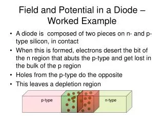
p-type n-type Field and Potential in a Diode – Worked Example • A diode is composed of two pieces on n- and p-type silicon, in contact • When this is formed, electrons desert the bit of the n region that abuts the p-type and get lost in the bulk of the p region • Holes from the p-type do the opposite • This leaves a depletion region
Depletion region? Large numbers of positive donor atoms in a small volume Large numbers of negative acceptor atoms in a small volume Small numbers of extra holes in a large volume Small numbers of extra electrons in a large volume -ve charge +ve charge ≈Charge neutral ≈Charge neutral p-type n-type Depletion region
p-type n-type Gauss’s Law • òòD.ds = charge enclosed • Choose a Gaussian surface that looks like the diode
Gaussian surface x |D| Now position it carefully and move it! p-type n-type Depletion region No charge enclosed, no field, constant potential E=-ÑV,D=εE V x
Gaussian surface x |D| Now position it carefully and move it! p-type n-type Depletion region E=-ÑV,D=εE -ve charge enclosed,-ve field increasing,+ve potential V x
Gaussian surface x |D| Now position it carefully and move it! p-type n-type Depletion region +ve charge enclosed,-ve field decreasing,+ve potential E=-ÑV,D=εE V x
Gaussian surface x |D| Now position it carefully and move it! p-type n-type Depletion region equal –ve and +ve charge enclosed,no field, constant +ve potential E=-ÑV,D=εE V x
x |D| p-type n-type Depletion region E=-ÑV,D=εE Actually this shape with such a simplified model V x