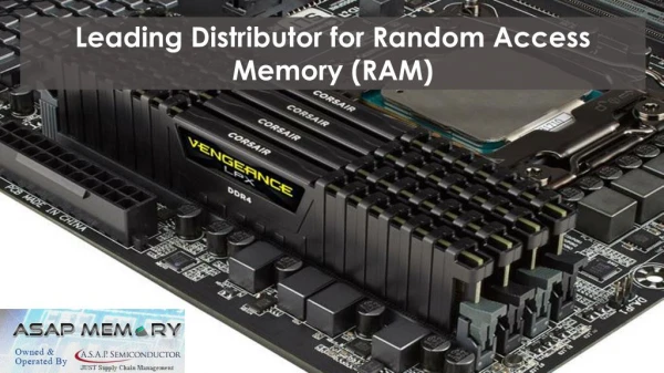
SDRAM Memory Controller
SDRAM Memory Controller. Static RAM Technology 6T Memory Cell Memory Access Timing Dynamic RAM Technology 1T Memory Cell Memory Access Timing. +. +. In X 0 1. OE_L 1 0 0. Out Z 0 1. IN. OUT. IN. OUT. OE_L. OE_L. OUT. OUT. OE_L. OE_L. IN. IN. 0. 0. Tri-State Gates.

SDRAM Memory Controller
E N D
Presentation Transcript
SDRAM Memory Controller • Static RAM Technology • 6T Memory Cell • Memory Access Timing • Dynamic RAM Technology • 1T Memory Cell • Memory Access Timing CS 150 - Fall 2005 – Lec #11: Memory Controller - 1
+ + In X 0 1 OE_L 1 0 0 Out Z 0 1 IN OUT IN OUT OE_L OE_L OUT OUT OE_L OE_L IN IN 0 0 Tri-State Gates CS 150 - Fall 2005 – Lec #11: Memory Controller - 2
Slick Multiplexer Implementation 2:1 Multiplexer IN0 OUT S 0 1 Out IN0 IN1 IN1 S CS 150 - Fall 2005 – Lec #11: Memory Controller - 3
Basic Memory Subsystem Block Diagram Address Decoder Word Line Memory cell 2n word lines what happensif n and/or m isvery large? n Address Bits m Bit Lines CS 150 - Fall 2005 – Lec #11: Memory Controller - 4
Static RAM Cell word 6-Transistor SRAM Cell • Write: • 1. Drive bit lines (bit=1, bit=0) • 2. Select row • Read: • 1. Precharge bit and bit to Vdd or Vdd/2 => make sure equal! • 2.. Select row • 3. Cell pulls one line low • 4. Sense amp on column detects difference between bit and bit word (row select) 0 1 0 1 bit bit bit bit replaced with pullup to save area CS 150 - Fall 2005 – Lec #11: Memory Controller - 5
Wr Driver & Precharger Wr Driver & Precharger Wr Driver & Precharger Wr Driver & Precharger - + - + - + - + - + - + - + - + Sense Amp Sense Amp Sense Amp Sense Amp Typical SRAM Organization: 16-word x 4-bit Din 3 Din 2 Din 1 Din 0 WrEn Precharge A0 Word 0 SRAM Cell SRAM Cell SRAM Cell SRAM Cell A1 Address Decoder A2 Word 1 SRAM Cell SRAM Cell SRAM Cell SRAM Cell A3 : : : : Word 15 SRAM Cell SRAM Cell SRAM Cell SRAM Cell Dout 3 Dout 2 Dout 1 Dout 0 CS 150 - Fall 2005 – Lec #11: Memory Controller - 6
A N 2 words N x M bit SRAM WE_L OE_L D M Logic Diagram of a Typical SRAM • Write Enable is usually active low (WE_L) • Din and Dout are combined to save pins: • A new control signal, output enable (OE_L) is needed • WE_L is asserted (Low), OE_L is disasserted (High) • D serves as the data input pin • WE_L is disasserted (High), OE_L is asserted (Low) • D is the data output pin • Both WE_L and OE_L are asserted: • Result is unknown. Don’t do that!!! CS 150 - Fall 2005 – Lec #11: Memory Controller - 7
A N 2 words N x M bit SRAM WE_L OE_L D M Typical SRAM Timing OE determines direction Hi = Write, Lo = ReadWrites are dangerous! Be careful! Double signaling: OE Hi, WE Lo Write Timing: Read Timing: High Z D Data In Data Out Data Out Junk A Write Address Read Address Read Address OE_L WE_L Write Hold Time Read Access Time Read Access Time Write Setup Time CS 150 - Fall 2005 – Lec #11: Memory Controller - 8
Problems with SRAM • Six transistors use up lots of area • Consider a “Zero” is stored in the cell: • Transistor N1 will try to pull “bit” to 0 • Transistor P2 will try to pull “bit bar” to 1 • Bit lines are already pre-charged high: Are P1 and P2 really necessary? Select = 1 P1 P2 Off On On On On Off N1 N2 bit = 1 bit = 0 CS 150 - Fall 2005 – Lec #11: Memory Controller - 9
1-Transistor Memory Cell (DRAM) • Write: • 1. Drive bit line • 2. Select row • Read: • 1. Precharge bit line to Vdd/2 • 2. Select row • 3. Cell and bit line share charges • Minute voltage changes on the bit line • 4. Sense (fancy sense amp) • Can detect changes of ~1 million electrons • 5. Write: restore the value • Refresh • 1. Just do a dummy read to every cell row select bit Read is really aread followed bya restoring write CS 150 - Fall 2005 – Lec #11: Memory Controller - 10
Classical DRAM Organization (Square) bit (data) lines • Row and Column Address together: • Select 1 bit a time r o w d e c o d e r Each intersection represents a 1-T DRAM Cell RAM Cell Array Square keeps the wires short: Power and speed advantages Less RC, faster precharge anddischarge is faster access time! word (row) select Column Selector & I/O Circuits Column Address row address data CS 150 - Fall 2005 – Lec #11: Memory Controller - 11
Memory Array DRAM Logical Organization (4 Mbit) Column Decoder 4 Mbit = 22 address bits 11 row address bits 11 col address bits • Square root of bits per RAS/CAS • Row selects 1 row of 2048 bits from 2048 rows • Col selects 1 bit out of 2048 bits in such a row … Data In D Sense Amps & I/O 11 R O W D E C O D E R Bit Line Data Out Q 11 A0…A10 Address Buffer (2,048 x 2,048) Storage W ord Line Cell CS 150 - Fall 2005 – Lec #11: Memory Controller - 12
Logic Diagram of a Typical DRAM • Control Signals (RAS_L, CAS_L, WE_L, OE_L) are all active low • Din and Dout are combined (D): • WE_L is asserted (Low), OE_L is disasserted (High) • D serves as the data input pin • WE_L is disasserted (High), OE_L is asserted (Low) • D is the data output pin • Row and column addresses share the same pins (A) • RAS_L goes low: Pins A are latched in as row address • CAS_L goes low: Pins A are latched in as column address • RAS/CAS edge-sensitive RAS_L CAS_L WE_L OE_L 256K x 8 DRAM D A 9 8 CS 150 - Fall 2005 – Lec #11: Memory Controller - 13
RAS_L DRAM READ Timing RAS_L CAS_L WE_L OE_L • Every DRAM access begins at: • Assertion of the RAS_L • 2 ways to read: early or late v. CAS D A 256K x 8 DRAM 9 8 DRAM Read Cycle Time CAS_L A Row Address Col Address Junk Row Address Col Address Junk WE_L OE_L D High Z Junk Data Out High Z Data Out Read Access Time Output Enable Delay Late Read Cycle: OE_L asserted after CAS_L Early Read Cycle: OE_L asserted before CAS_L CS 150 - Fall 2005 – Lec #11: Memory Controller - 14
Early Read Sequencing • Assert Row Address • Assert RAS_L • Commence read cycle • Meet Row Addr setup time before RAS/hold time after RAS • Assert OE_L • Assert Col Address • Assert CAS_L • Meet Col Addr setup time before CAS/hold time after CAS • Valid Data Out after access time • Disassert OE_L, CAS_L, RAS_L to end cycle CS 150 - Fall 2005 – Lec #11: Memory Controller - 15
Sketch of Early Read FSM Row Address to Memory FSM Clock? Setup time met? Assert RAS_L Hold time met? Assert OE_L, RAS_L Col Address to Memory Setup time met? Assert OE_L, RAS_L, CAS_L Hold time met? Assert OE_L, RAS_L, CAS_L Data Available (better grab it!) CS 150 - Fall 2005 – Lec #11: Memory Controller - 16
Late Read Sequencing • Assert Row Address • Assert RAS_L • Commence read cycle • Meet Row Addr setup time before RAS/hold time after RAS • Assert Col Address • Assert CAS_L • Meet Col Addr setup time before CAS/hold time after CAS • Assert OE_L • Valid Data Out after access time • Disassert OE_L, CAS_L, RAS_L to end cycle CS 150 - Fall 2005 – Lec #11: Memory Controller - 17
Sketch of Late Read FSM Row Address to Memory FSM Clock? Setup time met? Assert RAS_L Hold time met? Col Address to Memory Assert RAS_L Setup time met? Col Address to MemoryAssert RAS_L, CAS_L Hold time met? Assert OE_L, RAS_L, CAS_L Data Available (better grab it!) CS 150 - Fall 2005 – Lec #11: Memory Controller - 18
RAS_L DRAM WRITE Timing RAS_L CAS_L WE_L OE_L • Every DRAM access begins at: • The assertion of the RAS_L • 2 ways to write: early or late v. CAS A 256K x 8 DRAM D 9 8 DRAM WR Cycle Time CAS_L A Row Address Col Address Junk Row Address Col Address Junk OE_L WE_L D Junk Data In Junk Data In Junk WR Access Time WR Access Time Early Wr Cycle: WE_L asserted before CAS_L CS 150 - Fall 2005 – Lec #11: Memory Controller - 19 Late Wr Cycle: WE_L asserted after CAS_L
Key DRAM Timing Parameters • tRAC: minimum time from RAS line falling to the valid data output. • Quoted as the speed of a DRAM • A fast 4Mb DRAM tRAC = 60 ns • tRC: minimum time from the start of one row access to the start of the next. • tRC = 110 ns for a 4Mbit DRAM with a tRAC of 60 ns • tCAC: minimum time from CAS line falling to valid data output. • 15 ns for a 4Mbit DRAM with a tRAC of 60 ns • tPC: minimum time from the start of one column access to the start of the next. • 35 ns for a 4Mbit DRAM with a tRAC of 60 ns CS 150 - Fall 2005 – Lec #11: Memory Controller - 20
SDRAM Memory Controller • Static RAM Technology • 6T Memory Cell • Memory Access Timing • Dynamic RAM Technology • 1T Memory Cell • Memory Access Timing CS 150 - Fall 2005 – Lec #11: Memory Controller - 21