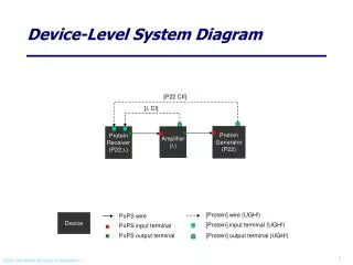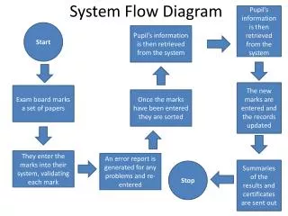
appliedVHDL System Context Diagram
170 likes | 205 Vues
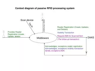
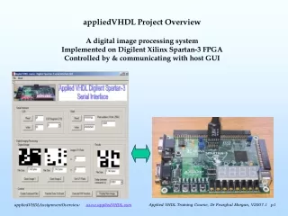
appliedVHDL Project Overview A digital i mage p rocessing s ystem Implemented on Digilent Xilinx Spartan-3 FPGA Controlled by & communicating with host GUI. appliedVHDL System Context Diagram. Top level process 0.0. DFD 0.0. Digilent Xilinx Spartan-3 Hardware Development Module.

appliedVHDL System Context Diagram
E N D
Presentation Transcript
appliedVHDL Project Overview A digital image processing systemImplemented on Digilent Xilinx Spartan-3 FPGA Controlled by & communicating with host GUI
appliedVHDL System Context Diagram Top level process 0.0 DFD0.0
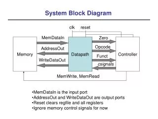
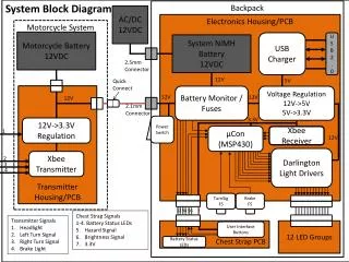
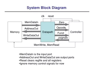
Digilent Xilinx Spartan-3 Hardware Development Module JTAG FPGA configuration bitstream download cable Voltage regulator 2Mbit platform flash config PROM FPGA config done LED VGA port Push button switch (forces FPGA reconfiguration) Expansion connectors Power In(& regulators) Xilinx Spartan-3 FPGA [XC3S200-4ft256] Poweronindicator LED PS/2 port Serial portRS-232 Four 7-segment displays [common led connections, separate anodes, all low asserted] 8 LEDs [ld(7:0)] Secondary oscillator skt 4 Push button switches [btn(3:0)] 8 Toggle Switches [sw(7:0)]
Digilent Spartan-3 Hardware Development ModulePCB Side 2 Voltage regulators 50Mhz Oscillator Two 256Kx16 SRAMs (can also be used as single 256Kx32 SRAM)
Host Serial Interface GUI • 6. Activate DSPBlk delta-frame gen (result written to SRAM Quadrant 2) • 7. Rdback processed image from SRAM. Convert to .bmpand display • Define serial txfrspeed (aids visual monitoring of serial data on FPGA dvp system 7-seg displays) • Direct SRAM r/w control • Direct CSR r/w control • Select/display B&W images. Define image size 4. Convert images to raw binary format 5. Transfer images to SRAM (Quadrants 0 & 1)
appliedVHDL Functions Host transfers command and data bytes to FPGA Using serial port. Control byte format : • rd/wr from/to 8 x byte-wide registers (CSRs) • Rd/wr from/to 256kx32-bit SRAM • Activate DSP function (e.g., image pixel subtraction) RW : 1=> read0 => write CSRTask RAM Task DSP Task RW unused csrAdd(2:0)
Control (and Status) Registers • Assume that appliedVHDL system includes 8xbyte-wide registers • which are used to configure the operation of the systemcsr(7)(7:0) : unused • csr(6)(7:0) : unused • csr(5)(7:0) : unused • csr(4)(7:0) : dspAddRange(15:8) • csr(3)(7:0) : dspAddRange(7:0) • csr(2)(7:0) : XXXXXX, IORamAdd(17:16) • csr(1)(7:0) : IORamAdd(15:8) • csr(0)(7:0) : IORamAdd(7:0) Used to control DSP function Used to define 18-bit SRAM address
CSR write Host transfers two bytes (1x control and 1x data) to FPGA Control byte format : Data byte : eg : Wr 56h to CSR(2) : byte 1=00100010, byte 2=01010110 Wr 23h to CSR(6) : byte 1=62h, byte 2=23h RW : 1=> read0 => write CSRTask RAM Task DSP Task RW unused csrAdd(2:0) Byte-wide data written to the addressed CSR
CSR read RW : 1=> read0 => write CSRTask RAM Task DSP Task RW unused csrAdd(2:0) Control byte : eg : rd CSR(4) : byte 1 = 01000011 = 43h
32-bit SRAM write RW : 1=> read0 => write CSRTask RAM Task DSP Task • Control byte : • SRAM address defined in CSR bytes (2:0). Requires 3 x CSR writes • eg : write 55667788h to RAM address 000004h Wr CSR(0), ram add (7:0) : 02h Data = 04h • Wr CSR(1), ram add (15:8) : 12h Data = 00h • Wr CSR(2), ram add (18:17) : 22h Data = 00h (XXXXXX00) • SRAM write instruction and 4 x RAM wr data bytes • Control byte (SRAM write) : 04h 4xdata bytes (Note :send LS Byte to FPGA first ): (LSB) 88h, 77h, 66h, 55h (MSB) • Serial byte sequence from host : 02 04 12 00 22 00 04 88 77 66 55 RW unused csrAdd(2:0)
32-bit SRAM read RW : 1=> read0 => write CSRTask RAM Task DSP Task • Control byte : • SRAM address defined in CSR bytes (2:0). Requires 3 x CSR writes • eg : read RAM address 32101h Wr CSR(0), ram add (7:0) : 02h Data = 01h • Wr CSR(1), ram add (15:8) : 12h Data = 21h • Wr CSR(2), ram add (18:17) : 22h Data = 03h (XXXXXX11) • SRAM read instruction control byte : 05h • Serial byte sequence from host : 02 01 12 21 22 03 05 RW unused csrAdd(2:0)
DSP FunctionDelta Image Processing A basic image pixel delta frame generation example is included in the appliedVHDL system A wide variety of DSP functions can be included, supported by CSR and SRAM resources, e.g., • Audio processing • Image processing • Encryption, coding algorithms • Games The appliedVHDL system can be extended to support other functions
DSP Delta Image Task Execution Image 0 in SRAM quadrant 0, image 1 in SRAM quadrant 1Quadrant size 64k 32-bit words Perform delta frame generation, i.e., (image 1 – image 0)Write result to SRAM quadrant 3 (same size as original images) SRAM Memory Map 11 1111 1111 1111 1111 (3FFFFh) 11 0000 0000 0000 0000 (30000h) 10 1111 1111 1111 1111 (2FFFFh) 10 0000 0000 0000 0000 (20000h)01 1111 1111 1111 1111 (1FFFFh) 01 0000 0000 0000 0000 (10000h) 00 1111 1111 1111 1111 (0FFFFh) 00 0000 0000 0000 0000 (00000h) Quadrant 3 Quadrant 2 Quadrant 1 Quadrant 0(64k x 32-bitlocations) max 64k x 32-bits 0044440 (delta result) FF8888FF (image 2 data longword) FF4444FF (image 1 data longword)
DSP Delta Image Task Execution Raw image format .bmp Image 1 : (4x4 pixels) (Black & White)Host converts .bmp to raw format and transfers to FPGA via serial port .bmp Image 2 : (4x4 pixels) Wr CSR(3) : 32h, data = 04h [dspAddRange(7:0)]Wr CSR(4) : 42h, data = 00h [dspAddRange(15:8)] C0FFC0FFFFCOFFCOC0FFC0FFFFCOFFCO Raw image format 00FF00FF FFC0FF0000FFC0FF FF0OFF0O
appliedVHDL Process 0.0 Description • PC-FPGA UART communication:From host to FPGA on signal RxD: - transfers serial command (8 bit value plus start/stop bits) - transfers serial data (8 bit value plus start/stop bits)From FPGA to host on signal TxD: - transfers serial data (8 bit value plus start/stop bits)UART IP core converts serial data to/from byte-wide data (UART core is provided by Xilinx) • FPGA waits for command from host and decodes host commandbytes - CSR acess (r/w) - SRAM access (r/w) - DSP activate
appliedVHDL Process 0.0 Description • Implements datapath : - Bundles byte-wide data bytes received in sequence from UART into 32-bit data for writing to SRAM. - Unbundles 32-bit data read from SRAM and transfer each byte to UART in sequence • Performs the following base-level tasks : - Control Register R/W : 8 x byte-wide registers (referred to as Control & Status Registers (CSRs) throughout) - Configure a number of control registers to define the SRAM 18-bit address - single 32-bit SRAM R/W data transfers
appliedVHDL Process 0.0 Description 5. Perform the following high-level task sequence : - Configure a number of control registers to support the required DSP function (image processing task) - Transfer two gray coded pixel images from host PC into SRAM quadrant 0 and quadrant 1 respectively, i.e., (image0 & image 1) - DSP task : perform delta image generation to the two images stored in RAM (image0 – image1) - Write resulting delta frame to RAM quadrant 2 - Transfer resulting image from SRAM quadrant 2 to the host PC for display 6. Display various signal and bus values on 7-segment display & LEDs