Update on Digital Board Status and Development Plan for FPGA Integration
150 likes | 262 Vues
This document details the current status of the Digital Board as of May 12, 2010, focusing on its operation with the PFDP Simulator, TDC, and Sweep/Deflector. It outlines minor circuit changes, a major implementation involving a daughter card for FPGA interconnects, and the primary digital board interconnects. The overview includes command and data flow testing, detailing how the GSE communicates with the FPGA via IDPU Simulator. The development plan emphasizes the use of a daughter card to enhance flexibility and minimize risks associated with non-reprogrammable components.

Update on Digital Board Status and Development Plan for FPGA Integration
E N D
Presentation Transcript
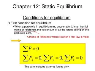
STATIC DIGITAL BOARD MAY 12, 2010 Rick Sterling
Digital Board Status • Engr Model working with PFDP Simulator, TDC, Sweep/Deflector • Minor changes to board circuits and parts for next version • Major change will be implementation of daughter card to carry the FPGA
Interconnect Overview • Primary Digital Board Interconnects • LVPS – wtax stackup • Sweep/Deflector – wtax • PFDPU • TDC – 2 x 20 • Anode – Test pulses
Command & Data Flow (Testing) • Data Flow • Generate start/stop at DG535 • 200 mV pulses to PreAmp • Amplified pulses to TDC • TOF and other data read by FPGA on digital board • Packetized data sent to GSE via IDPU Simulator. • Batch processing and display of data. • Command Flow • GSE sends command to FPGA via IDPU Simulator • FPGA issues appropriate control and goes to commanded configuration. • Example: Set threshold on TDC
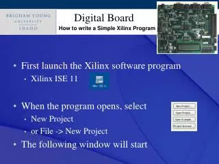
Daughter Card Strategy PLAN: Use Daughter Card to carry the FPGA and JTAG programming connector. This will interface to the mother board with Hypertronics’ HDLP (High Density Low Profile) connectors. RATIONALE: Overall: Minimize risk and maximize flexibility. WHY: Enable use of FLASH based FPGA as long as possible before going to non-reprogrammable fused part. Enable freezing of non FPGA design and layout early in process Enable changing FPGA without changing digital circuit mother board design and layout.
Overview: Mother and Daughter FPGA CG624: 1.28” x 1.28” HDLP-58: 0.30” x 1.30” JTAG: MicroHeader
Next Steps Put the entire STATIC instrument with source into the chamber and do end to end test. Implement and test daughter board interface with digital board.