Download
1 / 9
90 likes | 252 Vues
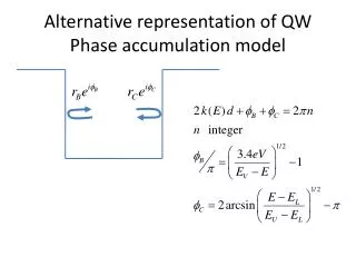
Alternative representation of QW Phase accumulation model. Dispersion of k(E). Synchrotron radiation photoemission spectroscopy. ISA Aarhus University Maximum Energy 580 MeV Max Current 250 mA Lifetime 15 hours. SGM1 30-400 eV 10 10 photons/sec @130 eV. Photoelectron spectroscopy.

E N D
Synchrotron radiation photoemission spectroscopy • ISA Aarhus University • Maximum Energy 580 MeV • Max Current 250 mA • Lifetime 15 hours • SGM1 • 30-400 eV • 1010 photons/sec @130 eV
Photoelectron spectroscopy • Core levels • Chemical reactions/mixing • Growth modes • Valence bands • Electronic levels relevant for optics
Wedge-shaped metal film AFM Sample moved into shadow of shield. Evaporation rate ~1 ML per minute Triangular domains ~200 nm Ag(111) LEED-pattern - only one type of domains Scanning film thickness by moving wedge through laser or synchrotron beam Width of synchrotron beam
Film growth - Si2p spectra Growth at 170 K leads to exponential decay of Si2p levels with ~5Å decay rate. Room temperature annealing of the film leads to growth of large atomically flat domains. Areas with low Ag coverage are formed. Annealing
Cu buffer layerCu wedge under 10-ML Ag film 3 ML Cu: disordered film 6-7 ML Cu: optimum for Ag overlayer > 7 ML Cu: coupling of overlayer and substrate levels - double peaks - avoided crossings
QW levels and film roughness 0 -0.5 -1 Binding Energy (eV) -1.5 Beam size on sample ~1 mm -2 -2.5 0 2 4 6 8 10 12 14 16 18 20 22 24 Thickness (ML) Film thickness variations expected within probed area Variations within a few atomic layer give broad peaks in photoemission