Download

1 / 18
180 likes | 296 Vues
Test of the MAPS add -on board. S. Amar-Youcef, M. Deveaux , D. Doering, C. Müntz , S. Seddiki , P. Scharrer, Ch . Schrader, J. Stroth , T. Tischler. Outline. Test setup Mi 20 – Sensor Data analysis Results : Test MAPS add -on board Summary.

E N D
Test ofthe MAPS add-on board S. Amar-Youcef, M. Deveaux, D. Doering, C. Müntz, S. Seddiki, P. Scharrer, Ch. Schrader, J. Stroth, T. Tischler
Outline • Test setup • Mi 20 – Sensor • Data analysis • Results: Test MAPS add-on board • Summary
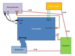
Test setupOnlyacquisitionboardchanged in contrasttoreferencesystem Mimosa20 (2008) Sensor Auxiliary board, power supply, signal processing, data transfer Frontend board (PCB) Test HADES-DAQ compatible, no dead time, big RAM space for data storage or buffering, 50MHz readout clock; Data processing: digitalization, sparsification Analog signals Sync. signals MAPS add-on board on TRB2 (TRBnet) Data transfer: I/O cardor OP-link Monitoring PC Analysis
Mimosa 20 - Sensor • Mimosa20 (2008): • Differential analog output • 2 banks • 10 submatrices • Multiplexed onto 2 outputs • 50 MHz • 200 kPixels • 30 µm pixel-pitch • SB pixels Rechargediode Output 30 µm Cparasitic Collectingdiode
Properties SB-pixel Potential atoutput: Equilibrium: Irecharge =Ileakage Rechargediode Output Irecharge CDS (Correlated Double Sampling): Ileakage Noise Cparasitic Potentiometer Collectingdiode
Chip slowcontrol • JTAG interfaceforchipsettings • Working pointofsourcefollower • Level markerpixels • Level ofsignals • Amplification • Analog buffer • Differential outputbuffer
Data analysissoftware Data takenandstored! Data Data Data Import ROOT Demultiplexing Hit-signal (Pixels overthreshold) Clusterfinding CDS Noise
Key observables: Kα (55Fe ) Gain Noise Histogramm Calibration [e-/ADC] Noise [e-] Noise in one Pixel Entries Pixel topixeldispersionof Noise Noise [ADC] Charge spectrumof 55-Fe source Noise [ADC]
Status on last collaborationmeeting • Goal: • Validatetheboard design • Check whetherwecanreachaspiredperformance • Maximizesensitivity ↔ minimizenoise • Understand MAPS add-on board in detail • Approach: • Systematicmeasurements • Optimizesettings Bachelor student: P. Scharrer • Wecouldstartrunningthissetupfor a first time • Readoutchainworkingproperly • But performanceof analoge electronics not clarified
ResultsCalibration: gain (@ f=50MHz) Eachdatapointmeasuredwith ‚optimal‘ settings! Dischargeof Kαsignal, due tohigherrechargecurrentathighertemperatures!
SB-Pixel: Potential atoutputwithhit: Irecharge < Ileakage + ISignal Irecharge = Ileakage Irecharge > Ileakage CDS: Hit-signal Athigherleakagecurrent: Pixel rechargefaster Hit signalsmaller
Calibration: gain (@ f=50MHz) Expectedsaturationvalue: 408 ADC = 1640 e-
Noise w.r.t. readoutfrequency: Resonant regionof MAPS add-on boards Conclusion: propertiesarecomparabletoreferencesystem The MAPS add-on boardisworking well!
Status now • Fullcontrolofthechip • Understand thebehaviourbytuningthe different parameters • Knowhowtobalancetheparameteragainsteachother in order tooptimizethenoise • Resultsmatchthe design goals
Summary Thankyou! • MAPS add-on board • Working well • Understand howtocontrolthe Mi20 with • Readyforbeamtime • Further steps: • Preparesetupandsoftwareforupcomingbeamtime
U-I – characteristicsofdiode: Non-linear behaviour