Download
1 / 1
20 likes | 208 Vues
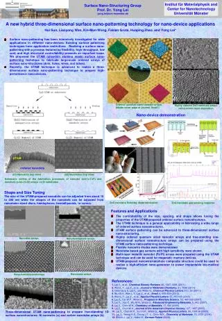
Nano-hemiellipsoid arrays. Nanoconic arrays. (b 2 ). (b 1 ). (a). UTAM. ordered nanodots. Nanodisc arrays. Nanohemisphere arrays. Three-dimensional UTAM nano-patterning to prepare free-standing 1D surface nanostructures: Ni nanowire (a) and carbon nanotube arrays (b).

E N D
Nano-hemiellipsoid arrays Nanoconic arrays (b2) (b1) (a) UTAM ordered nanodots Nanodisc arrays Nanohemisphere arrays Three-dimensional UTAM nano-patterning to prepare free-standing 1D surface nanostructures: Ni nanowire (a) and carbon nanotube arrays (b). Schematic outline of the fabrication processes of nanodot (a-b1-c1-d1) and nanohole (a-b2-c2-d2) arrays on Si substrates. (d1) Nanodots (top view) (d2) Nanoholes (top view) Institut für Materialphysik and Center for Nanotechnology Universität Münster Surface Nano-Structuring Group Prof. Dr. Yong Lei yong.lei@uni-muenster.de A new hybrid three-dimensional surface nano-patterning technology for nano-device applications Hui Sun, Liaoyong Wen, Kin-Mun Wong, Fabian Grote, Huaping Zhao, and Yong Lei* Surface nano-patterning has been intensively investigated for wide applications in different nano-devices. Existing surface patterning techniques have application restrictions . Realizing a surface nano-patterning with a process featured by flexibility, high throughput, low cost, and high structural controllability presents an important issue. We proposed the UTAM (ultra-thin alumina mask) surface nano-patterning technique to fabricate large-scale ordered arrays of surface nano-structures (dots, holes, wires, and tubes). Recently, the UTAM technique is advanced to realize a three-dimensional surface nano-patterning technique to prepare high-performance nano-devices. Ordered quantum-sized nanodot arrays (Inside cover page of Journal ‘Small’) Highly ordered ZnO nanotube arrays using atomic layer deposition Nano-device demonstration Shape and Size Tuning The size of the UTAM-prepared nanodots can be adjusted from about 10 to 200 nm while the shapes of the nanodots can be adjusted from nanometer-sized discs, hemispheres, hemiellipsoids, to conics. ZnO nanowire Schottky diode fabrication ZnO nanotube gas sensing response Features and Applications The controllability of the size, spacing, and shape allows tuning the properties of the UTAM-prepared ordered surface nanostructures. The UTAM technique is a general applicability in fabricating a wide range of ordered surface nanostructures. UTAM surface patterning can be advanced to three-dimensional surface nano-structuring. Highly ordered quantum sized nanodot arrays and free-standing one-dimensional surface nanostructure arrays can be prepared using the UTAM surface nano-patterning technique. Flexible nanowire diodes were demonstrated. Nanotube based gas sensors with high sensitivity were shown. Multi-layer metallic nanodot (Fe/Pt) arrays were prepared using the UTAM technique and can be used for magenetic memory devices. UTAM-prepared nanowire/nanohole composite structure could be used to realize a high-efficient nano-generator to power implantable bio-medical devices. References: 1.Lei Y., et al., Chemical Society Reviews, 40, 1247-1258 (2011). 2. Wen L.Y., Lei Y., et al., Journal of Materials Chemistry, 21, 7090 (2011) 3. Ostendorp S, Lei Y., and Wilde G., Chemical Physics Letters, 513, 99 (2011). 4. Wu M.H., Wen L.Y., Lei Y., et al., Small, 6, 695-699 (2010). 5. Wen L.Y., Lei Y., et al., Applied Physics Letters, 97, 053106 (2010) 6.Lei Y., Cai W.P., Wilde G., Progress in Materials Science, 52, 465-539 (2007). 7.Lei Y., Jiao Z., Wu M.H., Wilde G., Advanced Engineering Materials, 9, 343 (2007). 8. Lei Y., Chim W.K., Chemistry of Materials, 17, 580 (2005). 9. Lei Y., Chim W.K., Journal of the American Chemical Society, 127, 1487 (2005). 10.Lei Y., Chim W.K., Sun H.P., Wilde G., Applied Physics Letters, 86, 103106 (2005). 11.Lei Y.,Yeong K.S., Thong J.T. L., Chim W.K., Chemistry of Materials, 16, 2757 (2004). 12. Ellrich J., Lei Y., Hahn H., German Patent (2009). (b)