Si-Strip Front-End Electronics Development and Status Report
Get an overview of Si-Strip Front-End Electronics (FEE) development focusing on analog front-end, data processing, ASIC technology, design kits status, planning, and organization. Learn about the architecture, analog derandomization, ADC integration, and digital processing prerequisites.

Si-Strip Front-End Electronics Development and Status Report
E N D
Presentation Transcript
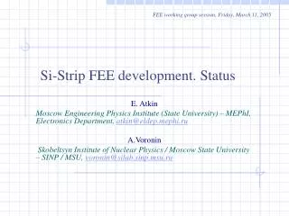
FEE working group session, Friday, March 11, 2005 Si-Strip FEE development. Status E. Atkin Moscow Engineering Physics Institute (State University) – MEPhI, Electronics Department,atkin@eldep.mephi.ru A.Voronin Skobeltsyn Institute of Nuclear Physics / Moscow State University– SINP / MSU, voronin@silab.sinp.msu.ru
Outline • View on FEE Structure development • What is between analog part and ADC? • Few analog FEE structures • Digital processing prerequisites • ASIC technology • Status on Design Kits • Planning and Organization: • People involved • Nearest plans I & II (2005-06) • Candidates for Sponsorship CBM Collaboration meeting, 9-11 March 2005, GSI
View on FEE Structure development “Each FEE channel consists of three parts: analog front-end, digitization plus digital back-end. The Strip FEE development is currently still in the first part of the conceptual design phase, where the design space is explored and the essential R&D issues are identified” (from TSR). The sketch given there supposes, that each channel has its own ADC. It is inefficient from the viewpoints of power consumption and chip area (cost). That forces us to develop the data driven architecture based on the technique of derandomization. Multichannel analog part ? Set of ADCs Figure 1 CBM Collaboration meeting, 9-11 March 2005, GSI
What is between analog part and ADC? (I) Analog derandomizer is a unit performing neuron-like processing, but in analog field. It is a deadtime free analog unit with n-inputs and m-outputs, n>m. Thus it allows to reduce the number of following ADCs. The derandomization procedure implies the skipping of empty channels and thus is indivisibly bound with data sparsification. Efficient processing of the randomly appearing signals by blocks, having a dead time, needs the choice of a proper architecture. Relevant references: • Design of a derandomizer with a buffer controller. University of Stockholm http://www.sysf.physto.se/kurser/digsyst/project1.html, 1999. • P. O’Connor, G. De Geronimo, A. Kandasamy. Amplitude and Time Measurement ASIC WithAnalog Derandomization: First Results. IEEE Trans. on NS, v. 50, N 4, 2003, p.892-897. CBM Collaboration meeting, 9-11 March 2005, GSI
What is between analog part and ADC? (II) Usually a derandomizer incorporates or is followed by such functional blocks as: • peak detectors (T&Hs) for amplitude measurement • TACs for time measurement • hit finder (fast low threshold LE discriminator) • arbitration logic • crosspoint switch • analog multiplexer CBM Collaboration meeting, 9-11 March 2005, GSI
Storage (T&H or PD) •bufferless deadtime • long readout time Preamps + Shapers Analog Storage + Analog Multiplex IN1 MUX IN2 ADC ● ● ● ● ● ● INn CLK Figure 2
Preamps +Shapers Multiple storage (interleavingT&H or PDs) Analogpipeline(SC memory) Preamps +Shapers Analog Memory + Analog Multiplex IN1 IN1 MUX MUX IN2 IN2 Multiple Storage Devices ADC ADC ● ● ● ● ● ● ● ● ● ● ● ● INn INn CLK CLK • buffered • long readout time • high power consumption •deadtimeless • complex control • long readout time Figure 3b Figure 3a
Analog storage devices (T&H or PD) Analog storage devices (T&H or PD) Crosspoint switch ADCs Crosspoint switch ADCs To DSP ● ● ● ● ● ● Address Address IN1 IN1 IN2 IN2 ● ● ● ● ● ● ● ● ● ● ● ● INn INn Arbitration Arbitration Preamps + Shapers Comparators Preamps + Shapers Comparators Figure 4b Crosspoint Switch One storage per channel Multiple storages shared by channels To DSP Figure 4a
Digital processing prerequisites (I) 8 Channels 40MHz ADC and 1280 MIPS DSP Module M.& A. Alyushin, Electronics Department, alyushin@eldep.mephi.ru CBM Collaboration meeting, 9-11 March 2005, GSI
Digital processing prerequisites (II) 64-Channels Block for 40MHz 10-bit ADC and 10240 MIPS DSP M.& A. Alyushin, Electronics Department, alyushin@eldep.mephi.ru CBM Collaboration meeting, 9-11 March 2005, GSI
ASIC Technology Status on Design Kits • Installed are (since Oct. 2004 meeting): • UMC CMOS 0.13 µm • AMIS CMOS 0.35 µm • Available are (not used yet): • IHP Si-Ge Bi-CMOS 0.25 µm • Thinking about (just installed): • UMC CMOS 0.18 µm as a main line for next 3-4 years according to TSR Jan.05 !!! We have some inertia in shifting our design flow from one process to another! In order to start the work of one design kit At least one person*month is needed! CBM Collaboration meeting, 9-11 March 2005, GSI
Planning and Organization in MEPhI: People involved • Electronics department M.Alyushin, E.Atkin, I.Ilyushchenko, A.Krasnuk, A.Silaev, Yu.Volkov+ 7 diploma students (2005/06) • Microelectronics department and Atomic and Accelerator radiation centers Yu.Bocharov, E.Onishchenko, V.Popov, A.Simakov • Department of Physics V.Emelianov Coordination: MEPhI Research director, prof. B.Bogdanovich CBM Collaboration meeting, 9-11 March 2005, GSI
Nearest plans I (2005/06) • Development of building blocks for data-driven architecture, according to UMC CMOS 0.18 µm. Prototyping via Europractice (MPW).These blocks are: • Preamp • Amplitude (slow) antialiasing and dynamic range saving shaper • Timing (fast), hit defining shaper • Low offset high-speed comparator both for hit finder and ADC. Studying both clocked and non-clocked options • Threshold DAC (6-8 bit) • Fast low-bit (4…6 or 8 bit ?) ADC • Analog Derandomizer (deadtime free analog unit with n-inputs and m-outputs, n>m) • Rail-to-rail op amp (high speed buffer) Common issues are: low power consumption, reasonable speed & chip area CBM Collaboration meeting, 9-11 March 2005, GSI
Nearest plans II (2005/06) • Design and production (via MPW) of a test purpose chip for SST prototyping, according to AMIS CMOS 0.35 µm rules Issues are: face-to-face interface to Si strip prototype, cost effective design • Lab tests of ICs manufactured • Radiation hardness tests of ICs • Development of FPGA based digital processing prototype CBM Collaboration meeting, 9-11 March 2005, GSI
Candidates for Sponsorship (2005/06) • ISTC • Russian Ministry on Education and Science • INTAS • FP7 (CORDIS) • other … CBM Collaboration meeting, 9-11 March 2005, GSI