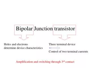
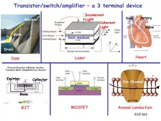
Transistor/switch/amplifier – a 3 terminal device
Transistor/switch/amplifier – a 3 terminal device. Incoherent Light. Artery. Vein. Source. Coherent Light. Valve. Gate. Gain medium. Drain. Heart. Laser. Dam. Emitter. Collector. Ion Channel. Base. MOSFET. Axonal conduction. BJT. All of these share a feature with….

Transistor/switch/amplifier – a 3 terminal device
E N D
Presentation Transcript
Transistor/switch/amplifier – a 3 terminal device Incoherent Light Artery Vein Source Coherent Light Valve Gate Gain medium Drain Heart Laser Dam Emitter Collector Ion Channel Base MOSFET Axonal conduction BJT ECE 663
All of these share a feature with… • Output current can toggle between large and small • (Switching Digital logic; create 0s and 1s) • Small change in ‘valve’ (3rd terminal) creates Large • change in output between 1st and 2nd terminal • (Amplification Analog applications; Turn 0.5 50)
Example: BJT common emitter characteristics Gain = 300
http://www.computerhistory.org/semiconductor/timeline.html#1940shttp://www.computerhistory.org/semiconductor/timeline.html#1940s
Aim of this chapter • How can we get ‘Gain’? • What is the structure of the device to get gain? • What is the equation for gain? • How can we use this equation to maximize gain? • How can we model this device as a circuit element? • What are its AC characteristics and speed?
Recall p-n junction P N N P W W + - - + Vappl < 0 Vappl > 0 Forward bias, + on P, - on N (Shrink W, Vbi) Allow holes to jump over barrier into N region as minority carriers Reverse bias, + on N, - on P (Expand W, Vbi) Remove holes and electrons away from depletion region I I V V
So if we combine these by fusing their terminals… P N N P W W + - - + Vappl < 0 Vappl > 0 • Holes from P region (“Emitter”) of 1st PN junction • driven by FB of 1st PN junction into central N region (“Base”) • Driven by RB of 2nd PN junction from Base into P region of • 2nd junction (“Collector”) • 1st region FB, 2nd RB • If we want to worry about holes alone, need P+ on 1st region • For holes to be removed by collector, base region must be thin
Bipolar Junction Transistors: Basics - + IC IE + - IB IE = IB + IC ………(KCL) VEC = VEB + VBC ……… (KVL)
BJT configurations GAIN CONFIG ECE 663
Bipolar Junction Transistors: Basics - + IC IE + - IB VEB >-VBC > 0 VEC > 0 but small IE > -IC > 0 IB > 0 VEB, VBC > 0 VEC >> 0 IE, IC > 0 IB > 0 VEB < 0, VBC > 0 VEC > 0 IE < 0, IC > 0 IB > 0 but small ECE 663
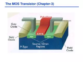
BJT Fabrication ECE 663
PNP BJT Electrostatics ECE 663
PNP BJT Electrostatics ECE 663
PNP Transistor Active Bias Mode VEB > 0 VCB > 0 Few recombine in the base Collector Fields drive holes far away where they can’t return thermionically Most holes diffuse to collector Large injection of Holes ECE 663
Forward Active minority carrier distribution P N P+ pB(x) nE(x’) nE0 pB0 nC0 nC(x’’) ECE 663
PNP Physical Currents ECE 663
PNP transistor amplifier action IN (small) OUT (large) Clearly this works in common emitter configuration ECE 663
Emitter Injection Efficiency - PNP IE IC ICp IEp C E IEn ICn IB Can we make the emitter see holes alone? ECE 663
Base Transport Factor IE IC ICp IEp C E IEn ICn IB Can all injected holes make it to the collector? ECE 663
Common Base DC current gain - PNP Common Base – Active Bias mode: IC = aDCIE + ICB0 ICp = aTIEp = aTgIE aDC = aTg IC = aTgIE + ICn ECE 663
Common Emitter DC current gain - PNP Common Emitter – Active Bias mode: IC IB IE = bDCIB + ICE0 IE bDC = aDC /(1-aDC) IC = aDCIE + ICB0 = aDC(IC + IB) + ICB0 GAIN !! IC = aDCIB + ICB0 1-aDC ECE 663
Common Emitter DC current gain - PNP Thin base will make aT 1 Highly doped P region will make g 1 ECE 663