Summery Before Mid-Semester Exam
250 likes | 461 Vues
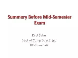
Summery Before Mid-Semester Exam. Dr A Sahu Dept of Comp Sc & Engg . IIT Guwahati. Outline. 8085 & 8086 Architectures Peripheral Devices Display, Keyboard, Data Converter Combined Peripheral controller + timer (8155) Peripheral Controller Peripheral Controller (8255)

Summery Before Mid-Semester Exam
E N D
Presentation Transcript
Summery Before Mid-Semester Exam Dr A Sahu Dept of Comp Sc & Engg. IIT Guwahati
Outline • 8085 & 8086 Architectures • Peripheral Devices • Display, Keyboard, Data Converter • Combined Peripheral controller + timer (8155) • Peripheral Controller • Peripheral Controller (8255) • Interrupt Controller (8259) • DMA Controller (8237) • Serial Communication controller (8251A) • Programmable Interval Timer (8254)
Mid Semester Exam • One page Data sheet of All Controller will be provided • Architecture, Control word, Status word, Mode • 8155 iot, 8255ioc, 8259pic, 8237dma, 8251usart, 8254pit • 5 questions (Order may be different) • 2 Theory and Concepts • (40 % Easy) • 2 Design question • (40 % can be done easily if u have attend the class) • 1 Thinking question • (20% ; relatively top level) • Timing & Venue: • 10.00AM-12.00Nn, 20 Sept 2010, 2202/2204
8085 Microprocessor Architecture ReSeT6.5 INTR TRAP INTA RST5.5 RST7.5 SID SOD Interrupt Control Serial I/O Control Bus 8 Bit MUX ACC tmp R IR W Z B C Flag D E I Decode & M/C Encoding ALU H L SP PC Inc/Dec. ter Add latch Timing and Control Add Buff Data/Add Buff
8086 Architecture Bus Interface Unit C BUS AH AL SUM BH BL Q6 Q5 CH CL Q4 Q3 DH DL Q2 Q1 SI (Source Idx ) DI (Dest. Idx) BP (Base Ptr ) Sequencer SP (Stack Ptr) Execution Unit A BUS CS (Code SegReg) DS (Data SegReg ) Temp A Temp B ES (Extra SegReg ) Temp C SS (Stack SegReg) IP (IntrPtr) ALU Operand Z (Flag Reg) InDirect
8086 Registers • AX - the accumulator register (divided into AH / AL) • BX - the base address register (divided into BH / BL) • CX - the count register (divided into CH / CL) • DX - the data register (divided into DH / DL) • SI - source index register. • DI - destination index register. • BP - base pointer. • SP - stack pointer. AH AL BH BL CH CL DH DL SI (Source Idx ) DI (Dest. Idx) BP (Base Ptr ) SP (Stack Ptr) Z (Flag Reg) CS (Code SegReg) DS (Data SegReg ) ES (Extra SegReg ) SS (Stack SegReg) IP (IntrPtr)
Memory layout of C program int A; int B=10; main(){ intAlocal; int *p; p=(int*)malloc(10); } Stack Heap Data BSS Code
MASM : Hello world .model small .stack 100h ; reserve 256 bytes of stack space .data message db "Hello world, I'm learning Assembly$” .code main proc mov ax, seg message ; ax<-data seg. start addr. movds, ax ; Initialize SegReg mov ah, 09 ; 9 in the AH reg indicates Procedure ;hould write a bit-string to the screen. lea dx, message ;Load Eff Address int 21h mov ax,4c00h ; Halt for DOS routine (Exit Program) int 21h main endp end main
GetChar, PutChar • putchar( ‘a‘ ) ; • c = getchar() ; mov dl, ‘a‘ ;dl = ‘a‘ mov ah, 2h ;character output subprogram int 21h ; call ms-dos output character mov ah, 1h ; keyboard input subprogram int 21h ; char input, char is stored in al mov c, al ; copy character from al to c
Transmission controller • Transmission Controller: • MPU control, Device Control (DMA) • Type of IO mapping • Peripheral (IN/Out), Memory mapped IO (LD/ST,MV) • Format of communication • Synchronous (T & R sync with clock), Asynchronous • Mode of Data Transfer • Parallel, Serial (UART) • Condition for data transfer • Uncond., Polling, Interrupt, Ready signal, Handshake
D/A converter FS 7 • FullScaleOutput=(FullScaleValue – 1LSBValue) • 1MSB Value=1/2 * FSV 6 Digital to Analog Converter D2 LSB 5 Vo 4 Analog output D1 Analog Output 3 2 D0 1 0 000 001 010 011 100 101 110 111 Digital Inputs • Resolution, Reference Voltages, Settling Time, Linearity, Speed, Errors
A/D Conversion Techniques • Counter or Tracking ADC • Successive Approximation ADC • Most Commonly Used • Parallel or Flash ADC • Fast Conversion
Display 7 Seg 9 Seg 16 Seg 3x5 DotMatix 5x7 9x11 Dot Matrix Display Panel 25x80 character monitor
Multiplexed line and Memory use 40 Bit data line Data 0 2 1 3 4 0 Mod 5 Counter Data 1 Data 2 Data 3 Data 4 8 Bit data line
Multiplexed 25x80 Char Display Row Ctr Col Ctr CLK > 50Hzx25x80 0 1 2 3 4 ….. 78 79 0 1 2 23 24 C A T F I R E Decoder Or ROM Memory 25x80 character monitor Decoded Bits A
Multiplexed 1024x768 pixel display Row Ctr Col Ctr CLK > 1024x768x50Hz 0 1 2 3 4 ….. …1023 0 1 2 767 Frame Buffer 1024x768 Pixel LCD 8x3=24 Bits R B G Refresh screen 50 time a Sec
How Keyboard work ? ==1D +5V 14 15 1 3 0 2 . . . N to Lg(n) decoder A B C D 0 0 1 1
Simple keyboard with 64 keys C2 C6 C7 C0 C1 • Scan Row (6) • Scan Column (3) • Send this to Decoder to generate ASCII value or Scan code R0 Scan Row R6 R1 Decode to ACSII (Memory ROM) To Host (CPU) R2 R6 6,3 R7 Scan Col: C2
8155 IO/Timer • D0, D1: mode for PA and PB, 0=IN, 1=OUT • D2, D3: mode for PC • D4, D5: interrupt EN for PA and PB, 0=disable 1=enable • D6, D7: Timer command: • 00: No effect • 01: Stop if running else no effect • 10: Stop after terminal count (TC) if running, else no effect • 11: Start if not running, reload at TC if running. • Port C bits (D2, D3) CEb CWR • M2, M1: mode bits: • 00: Single square wave of wavelength TC/2 (TC/2,TC/2 if TC even; [TC+1/2],[TC-1/2] if TC odd) • 01: Square waves of wavelength TC (TC/2,TC/2 if TC even; [TC+1/2],[TC-1/2] if TC odd) • 10: Single pulse on the TC'th clock pulse • 11: Single pulse on every TC'th clock pulse. Latch Port A AD0-AD7 A0-A7 PA0-PA7 3 to 8 Decoder Port B 0 1 2 3 4 5 ALE A2 PB0-PB7 D7-D0 A1 Port C A0 PC0-PC5 Timer MSB LSB Timer Out Clock for timer
7 6 5 4 3 2 1 0 D7 D6 D5 D4 D3 D2 D1 D0 Group B Port C(L) – 1 Input 0 output Port B – 1 Input 0 output Mode select: 0 mode 0; 1 mode 1 Port C(U) – 1 Input 0 output Port A – 1 Input 0 output Mode select: 00 mode 0; 01 mode 1; 1x mode 2 1 – mode select 0 – bit set/reset Group A 8255 PPC Gr A Port A (8) I/O PA7-PA0 D7 D6 D5 D4 D3 D2 D1 D0 0/1 Group A Control I/O Mode BSR Mode Bit Set/Reset Bi directional Data Bus D7-D0 I/O PC7-PC4 Gr A Port C (H 4) BSR Mode Bit Set/Reset For Port C No Effect on I/O Mode Mode 0 Simple I/O for Ports A, B & C Mode 1 HS mode for Ports A and/or B Port C bits are used for HS Mode 2 Bidirectional Data mode for PortA B can in mode 0/1 Port C bits are used for HS Data Bus Buffer Gr B Port C (L 4) I/O PC3-PC0 8 bit Internal Data Bus Read Write Control Logic RDb WRb A1 A0 RESET CSb Group B Control Gr B Port B (8) I/O PB7-PB0
8259 PIC INTAb INT Internal Bus Control Logic 8259A Programmable Interrupt Controller IRQ0 8 bit Data Bus RDb WRb CSb A0 INT INTAb SPb/ENb IRQ1 IRQ0 IRQ1 IRQ2 IRQ3 IRQ4 IRQ5 IRQ6 IRQ7 Interrupt Service Register Priority Resolver Interrupt Request Register IRQ2 IRQ3 IRQ4 IRQ5 Interrupt Mask Register IRQ6 IRQ7
8237 DMA A7 A6 A5 A4 IO/Mb 3 to 8 Decoder CSb To data Bus DB0-DB7 A0-A3 A4-A7 00 DMA Req0 DMA Req 1 DMA Req 2 DMA Req 3 DREQ0 DREQ1 DREQ2 DREQ3 RegAddr Meaning DREQ0 A3 A2 A1 A0 To Address Bus 00 CH0 memory Add reg DREQ1 01 CH0 Count reg DREQ2 DREQ3 02 CH1 memory Add reg ADSTB HOLD Address Strobe Hold request DMA ack0 DMA ack1 DMA ack2 DMA ack3 IO Read I/O Write Memory Read Memory Write End of Process 03 CH1 Count reg A4-A7 04 CH2 memory Add reg DACK0 05 CH2 Count reg DB7-DB0 DACK0 DACK1 DACK2 DACK3 CMD DACK1 Hold Ack Clock Reset Ready Chip Select HLDA 06 CH3 memory Add reg ADSTB DACK2 07 CH3 Count reg AEN DACK3 08 R/W status/Commndreg MEMRb 09 WR request reg CLK 10 WR Single mask reg MEMWb Mode 11 WR mode reg IORb RESET READY IORDb IOWRb MemRDb MemWRb 12 WR Clear byte ptr F/F Mask IOWb Req 13 R/W Master Clear/Temp EOP 14 WR Clear Mask Reg READY RESET 15 WR all Mask clear bits CSb CLK HRQ Status EOPb HLDA
DSR SYN DET FE OE PE Tx EMPTY RxRDY TxRDY 8251 USART Internal Line Data Bus Buffer Transmit Buffer TXD D7-D0 EH D7 IR D6 D5 RTS ER D4 SBRK D3 RxE D2 D1 DTR D0 TxE RESET CLK C/Db RDb WRb CSb R/W Control Logic TXRDY TXE TXC Transmit Control TxE: transmit enable (0/1 Enable Disable) DTR: data terminal ready (1=ENABLE DTR) RxE: receiver enable (1/0=EN/DISABLE) SBPRK: send break character 1= force TxD low ER: error reset (Reset Flags: Parity ,Over run, Framing Error of Status Word) RTS: request to send (1= Enable Request to send) IR: internal reset (Reset 8251 to mode) EH: enter hunt mode (1=search for Sync Character) TxRDYtransmit ready (DB Buffer is empty) RxRDY receiver ready TxEMPTY transmitter empty PEparity error (1=when PE detected) OEoverrun error FEframing error (Aynsc only, Valid stop bit not detected) SYNDET sync. character detected DSRdata set ready (DSR set at 0 level) Framing Control # of Stop bits Character length Baud Rate 00: invalid 01: 1 bit 10: 1.5 bits 11: 2 bits DSRb DTRb CTSb RTSb Modem Control Receive Buffer RXD 00: Syn. Mode 01: x1 clock 10: x16 clock 11: x64 clock 00: 5 bits 01: 6 bits 10: 7 bits 11: 8 bits Parity Control X0=No Parity 01: Even 11: Odd Receive Control RXRDY RXC SYBDET
8254 PIT • Mode 0 : Interrupt on Terminal count • Mode 1 : Hardware Retriggerable One Shot • Mode 2 : Rate Generator • Mode 3 : Square wave generator • Mode 4 : Software Triggered Strobe • Mode 5 : Hardware Triggered Strobe Internal Bus D0-D7 Data Bus Buffer Counter 0 CLK 0 GATE 0 OUT 0 RDb WRb A0 A1 CSb Read/ Write Logic Counter 1 CLK 1 GATE 1 OUT 1 Counter 2 CLK 2 GATE 2 OUT 2 Control Word Register
Thanks & Good Luck for your Exam