Peripheral Devices and Input-Output Organization
Learn about peripheral devices, I/O organization, data transfer modes, priority interrupts, and more in a computer system setup. Explore the functionalities of keyboards, displays, printers, and other peripherals in the I/O subsystem.

Peripheral Devices and Input-Output Organization
E N D
Presentation Transcript
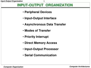
INPUT-OUTPUT ORGANIZATION • Peripheral Devices • Input-Output Interface • Asynchronous Data Transfer • Modes of Transfer • Priority Interrupt • Direct Memory Access • Input-Output Processor • Serial Communication
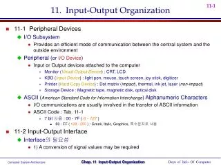
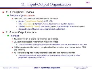
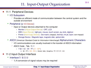
The input output subsystem of a computer, referred to as I/O, provides an efficient mode of communication between the central system and the outside environment. Input output devices attached to the computer are called as peripherals. Among the common peripheral are keyboards, mouse, display units, and printers etc. Peripherals that provide auxiliary storage for the systems are magnetic disks and tapes. Peripherals are electromechanical and electromagnetic devices. Peripheral Devices
Devices that are under the direct control of the computer are said to be connected on-line. These devices are designed to read information into or out of the memory unit upon command from the CPU and are considered to be part of the total computer system. The data transfer rate of peripheral devices differ from each other. Each peripheral behaves differently from any other. The input-output organization of a computer is a function of the size of the computer and the devices connected to it. Peripheral Devices
ASCII Alphanumeric Characters: I/O Devices that communicate with people and the computer are usually involved in the transfer of alphanumeric information to and from the device and the computer. The standard binary code for the alphanumeric characters is ASCII (American Standard Code for Information Interchange). Peripheral Devices
American Standard Code for Information Interchange b7 b6 b5 1 0 0 0 1 0 0 1 1 1 0 1 1 1 0 0 0 1 0 0 0 1 1 1 b4 b3 b2 b1 0 0 0 0 0 0 0 1 0 0 1 0 . . . . . . . . . . . . 1 1 1 0 1 1 1 1
Peripheral Devices PERIPHERAL DEVICES Input Devices Output Devices • Keyboard • Optical input devices • - Card Reader • - Paper Tape Reader • - Bar code reader • - Digitizer • - Optical Mark Reader • Magnetic Input Devices • - Magnetic Stripe Reader • Screen Input Devices • - Touch Screen • - Light Pen • - Mouse • Analog Input Devices • Card Puncher, Paper Tape Puncher • CRT • Printer (Impact, Ink Jet, • Laser, Dot Matrix) • Plotter • Analog • Voice
Provides a method for transferring information between internal storage (such as memory and CPU registers) and external I/O devices. I/O devices needs special communication links for interfacing them with the CPU. The purpose of the communication link is to resolves the differences between the computer and peripheral devices. Input/Output Interfaces INPUT/OUTPUT INTERFACE
The major differences are:- (1) Peripherals – Electromechanical and electromagnetic Devices CPU or Memory - Electronic Device Therefore a conversion of signal values may be required. (2) Data Transfer Rate Peripherals - Usually slower CPU or Memory - Usually faster than peripherals Some kinds of Synchronization mechanism may be needed (3) Unit of Information Peripherals – Byte, Block, … CPU or Memory – Word (4) Data representations may differ. (5) Operating mode of peripherals are differ from each other and each must be controlled so as not to disturb the operation of others peripherals connected to the CPU. To resolve these differences, computer system includes special hardware components between CPU and I/O devices to supervise and synchronize all input and output transfers. These components are called interface units. Input/Output Interfaces INPUT/OUTPUT INTERFACE
Input/Output Interfaces I/O BUS AND INTERFACE MODULES I/O bus Data Processor Address Control Interface Interface Interface Interface Keyboard Magnetic Magnetic and Printer disk tape display Each peripheral has an interface module associated with it interface with do following: terminal • - Decodes the device address (device code) • - Decodes the commands (operation) • - Provides signals for the peripheral controller • Synchronizes the data flow and supervises the transfer rate • between peripheral and CPU or Memory Typical I/O instruction Op. code Function code Device address (Command)
The I/O bus from the processor is attached to all the I/O devices interface. To communicate with a particular device, the processor puts a device address on the address line. When interface detects its own address, it activate the path between the bus line and the device that it controls. At the same time that the address is made available in the address lines, the processor provides a function code in the control lines. Commands
The interface selected respond to the function code and proceeds to execute it. The function code is referred to as an I/O command and is in essence an instruction that is executed in the interface and its attached peripheral unit. There are four types of command that an interface may receive. Control, Status, Data Output, Data Input. Commands
Input/Output Interfaces CONNECTION OF I/O BUS Connection of I/O Bus to CPU Computer Op. Device Function Accumulator I/O register code address code control CPU Sense lines Data lines I/O bus Function code lines Device address lines Connection of I/O Bus to One Interface Data lines Peripheral register Buffer register Device address Output peripheral I/O bus device AD = 1101 Interface Logic and controller Function code Command decoder Sense lines Status register
Input/Output Interfaces I/O BUS AND MEMORY BUS • In addition to communicating with I/O, • the processor must communicate with • the memory unit. • Like the I/O bus, the memory bus contains • data, address, and read/write control lines. • Functions of Buses • MEMORY BUS is for information transfers • between CPU and the MM • I/O BUS is for information transfers between • CPU and I/O devices through their I/O interface
Input/Output Interfaces I/O BUS AND MEMORY BUS Physical Organizations • Many computers use a common single bus • system for both memory and I/O interface units. • Use one common bus but separate control • lines for each function • Use one common bus with common control • lines for both functions • Some computer systems use two separate • buses • *one to communicate with memory and • *the other with I/O interfaces
Input/Output Interfaces ISOLATED vs MEMORY MAPPED I/O Isolated I/O - Separate I/O read/write control lines in addition to memory read/write control lines - Separate (isolated) memory and I/O address spaces - Distinct input and output instructions
Input/Output Interfaces ISOLATED vs MEMORY MAPPED I/O Memory-mapped I/O • - A single set of read/write control lines • (no distinction between memory and I/O • transfer) • - Memory and I/O addresses share the common address space • -> reduces memory address range available • - No specific input or output instruction • -> The same memory reference instructions can be used for I/O transfers • - Considerable flexibility in handling I/O operations
Input/Output Interfaces I/O INTERFACE I/O data Port A register Bidirectional Bus data bus buffers I/O data Port B register I/O Device CPU Chip select CS Internal bus Register select Control Control RS1 Timing register Register select and RS0 Control I/O read RD Status Status I/O write register WR The I/O data to and from the device can be transferred into either port A or port B. CS RS1 RS0 Register selected 0 x x None - data bus in high-impedence 1 0 0 Port A register 1 0 1 Port B register 1 1 0 Control register 1 1 1 Status register The transfer of data, control, or status information is via a common data bus. The distinction between data, control, or status information is determine from the particular interface register with which the CPU communicates.
Asynchronous Data Transfer ASYNCHRONOUS DATA TRANSFER Synchronous and Asynchronous Transfer Operations Synchronous – All devices derive use the timing information from common clock line Asynchronous – No common clock used. All devices derive use timing information from own clock.
Asynchronous Data Transfer ASYNCHRONOUS DATA TRANSFER • Asynchronous Data Transfer • Asynchronous data transfer between two independent units requires that control signals be transmitted between the communicating units to indicate the time at which data is being transmitted. • One way to achievingthis is by means of a STROBE pulse method. • Other way is HANDSHAKING method. • In general case we consider the transmitting unit as the source and receiving unit as the destination.
Strobe pulse - A strobe pulse is supplied by one unit to indicate the other unit when the transfer has to occur. Handshaking - A control signal is accompanied with each data being transmitted to indicate the presence of data. - The receiving unit responds with another control signal to acknowledge receipt of the data. Asynchronous Data Transfer Methods
Asynchronous Data Transfer STROBE CONTROL * Employs a single control line (STROBE) and a data bus . * The strobe may be activated by either the source or the destination unit. Source-Initiated Strobe for Data Transfer Destination-Initiated Strobe for Data Transfer Block Diagram Block Diagram Data bus Data bus Source Destination Source Destination unit unit unit unit Strobe Strobe Timing Diagram Timing Diagram Valid data Valid data Data Data Strobe Strobe
Asynchronous Data Transfer HANDSHAKING In Strobe Methods - Source-Initiated -The source unit that initiates the Transfer has no way of knowing whether the destination unit has actually received data. Destination-Initiated - The destination unit that initiates the transfer no way of knowing whether the source has actually placed the data on the bus. * To solve this problem, the HANDSHAKE method introduces a second control signal to provide a Reply to the unit that initiates the transfer.
Asynchronous Data Transfer SOURCE-INITIATED TRANSFER USING HANDSHAKE Data bus Source Data valid Destination Block Diagram unit unit Data accepted Valid data Data bus Timing Diagram Data valid Data accepted Sequence of Events Destination unit Source unit Place data on Data bus. Enable data valid. Accept data from bus. Enable data accepted Disable data valid. Invalidate data on bus. Disable data accepted. Ready to accept data (initial state). * Allows arbitrary delays from one state to the next * Permits each unit to respond at its own data transfer rate * The rate of transfer is determined by the slower unit
Asynchronous Data Transfer DESTINATION-INITIATED TRANSFER USING HANDSHAKE Data bus Block Diagram Source Data valid Destination unit unit Ready for data Timing Diagram Ready for data Data valid Valid data Data bus Sequence of Events Destination unit Source unit Ready to accept data. Enable ready for data. Place data on bus. Enable data valid. Accept data from bus. Disable ready for data. Disable data valid. Invalidate data on bus (initial state).
HANDSHAKING • Handshaking provides a high degree of flexibility and reliability because the successful completion of a data transfer relies on active participation by both units. • If one unit is faulty, data transfer will not be completed -> Can be detected by means of a timeout mechanism, which produces a alarm if data transfer is not completed in time.
Asynchronous Data Transfer ASYNCHRONOUS SERIAL TRANSFER Asynchronous serial transfer Synchronous serial transfer Asynchronous parallel transfer Synchronous parallel transfer Four Different Types of Transfer :->>> Asynchronous Serial Transfer - Employs special bits which are inserted at both ends of the character code - Each character consists of three parts; Start bit; Data bits; Stop bits. 1 1 0 0 0 1 0 1 Stop Start Character bits bit (1 bit) bits (at least 1 bit) A character can be detected by the receiver from the knowledge of 4 rules; - When data are not being sent, the line is kept in the 1-state (idle state) - The initiation of a character transmission is detected by a Start Bit , which is always a 0 - The character bits always follow the Start Bit - After the last bit of the character , a Stop Bit is detected when the line returns to the 1-state for at least 1 bit time
Consider the serial transmission of a terminal whose transfer rate is 10 character per second. Each transmitted consists of a start bit, eight information bits, and two stop bits, for a total of 11 bits. Ten character per second means that each character takes 0.1 second for transfer. Since there are 11 bits to be transmitted, it follows that the bit time is 9.09 ms. The baud rate is defined as the rate at which serial information is transmitted and is equivalent to the data transfer in bits per second. Ten character per second with an 11-bit format has a transfer rate of 110 baud. BAUD RATE
Asynchronous Data Transfer CS RS Oper. Register selected 0 x x None 1 0 WR Transmitter register 1 1 WR Control register 1 0 RD Receiver register 1 1 RD Status register UNIVERSAL ASYNCHRONOUS RECEIVER-TRANSMITTER - UART - A typical asynchronous communication interface available as an IC Parallel transformation It functions as both as a transmitter and receiver. Transmit data Transmitter Shift Bidirectional register data bus register Bus buffers Serial transformation Transmitter Control Transmitter clock register control and clock Chip select CS Internal Bus Register select Receiver Status Receiver RS Timing clock register control and I/O read and clock RD Control Receive I/O write WR data Receiver Shift register register Transmitter Register - Accepts a data byte(from CPU) through the data bus - Transferred to a shift register for serial transmission Receiver - Receives serial information into another shift register - Complete data byte is sent to the receiver register Status Register Bits - Used for I/O flags and for recording errors (parity , framing, overrun error) Control Register Bits - Define baud rate, no. of bits in each character, whether to generate and check parity, and no. of stop bits , used for initialization. Parallel transformation Serial transformation
FIFO buffer stores information in first in and first out manner. It can input data and out put data at two different rates. So it is useful when source and destination unit has different data transfer rates. Output data are always in the same order in which the data entered the buffer. Useful in some applications when data is transferred asynchronously FIRST-IN-FIRST-OUT(FIFO or Queue ) BUFFER
Asynchronous Data Transfer FIRST-IN-FIRST-OUT(FIFO) BUFFER 4 x 4 FIFO Buffer (4 4-bit registers R1,R2,R3,R4), store 4 words of four bits each. A Control Register (flip-flops Fi, associated with each Ri), Fi is set 1 indicates a 4-bit data word is stored in Ri, if Fi=0 means Ri not contain valid data. Control registers direct the movement of data through the registers. Whenever Fi=1 and the Fi+1 bit is reset (Fi’+1=1), a clock is generated Causing register R(i+1) to accept data from Ri. The same clock sets Fi+1 to 1 and reset Fi to 0. R1 R2 R3 R4 Data 4-bit 4-bit 4-bit 4-bit Data register input register register register output Clock Clock Clock Clock Insert S F S F F S S F F S S F 1 2 3 4 Destination-Initiated pair of Handshake lines Output ready F' F' F' F F' F' R R R R R R 4 1 2 3 Source-initiated pair of handshake lines Delete Input ready Master clear
Modes of Transfer MODES OF TRANSFER - PROGRAM-CONTROLLED I/O - 3 different Data Transfer Modes between the central computer(CPU or Memory) and peripherals; Program-Controlled I/O Interrupt-Initiated I/O Direct Memory Access (DMA) Program-Controlled I/O(Input Dev to CPU) Interface Data bus I/O bus Address bus Data register I/O Data valid CPU device I/O read Data accepted I/O write Status F register Read status register Polling or Status Checking Check flag bit • Continuous CPU involvement • CPU slowed down to I/O speed • Simple • Least hardware = 0 flag = 1 Read data register Transfer data to memory Transferring data under program control requires constant monitoring of the peripherals by the CPU.(CPU stays in a program loop). Useful for small low speed computers or in systems that are dedicated to monitor a device continuously. no Operation complete? yes Continue with program
Consider a typical computer that can execute the two instructions that read the status register and check the flag in 1 μs. Assume that the input device transfers its data at an average rate of 100bytes per second. This is equivalent to one byte every 10,000 μs. This means that the CPU will check the flag 10,000 times between each transfer. (Know as polling and status checking.) Example
Modes of Transfer MODES OF TRANSFER - INTERRUPT INITIATED I/O • Polling takes valuable CPU time • Open communication only when • some data has to be passed -> • Interrupt to the CPU. • I/O interface, instead of the CPU, • monitors the I/O device. • When the interface determines • that the I/O device is ready for • data transfer, it generates an • Interrupt Request to the • CPU.
Modes of Transfer MODES OF TRANSFER - INTERRUPT INITIATED I/O • Upon detecting an interrupt, CPU • stops momentarily the task it is doing, • branches to the service routine to • process the data transfer, and then • returns to the task it was performing. • CPU responds to the interrupt signal • by storing the return address from the • program counter into memory stack • and then control branches to a • service routine that processes the • required I/O transfer.
Modes of Transfer MODES OF TRANSFER - DMA DMA (Direct Memory Access) • Large blocks of data transferred • at a high speed to or from high • speed devices, magnetic drums, • disks, tapes, etc. • DMA controller is a Interface that • provides I/O transfer of data • directly to and from the memory • and the I/O device
Modes of Transfer MODES OF TRANSFER - DMA DMA (Direct Memory Access) • CPU initializes the DMA • controller by sending a memory address and the number of words to be transferred. • Actual transfer of data is done directly between the device and memory through DMA controller --> Freeing CPU for other tasks.
Priority Interrupt PRIORITY INTERRUPT Priority - Determines which interrupt is to be served first when two or more requests are made simultaneously - Also determines which device’s interrupts are permitted to interrupt the computer while another is being serviced - Higher priority interrupts can make requests while servicing a lower priority interrupt
Priority Interrupt PRIORITY INTERRUPT Priority Interrupt by Software(Polling) - Priority is established by the order of polling the devices (interrupt sources) - Flexible since it is established by software - Low cost since it needs a very little hardware - Very slow
Priority Interrupt PRIORITY INTERRUPT Priority Interrupt by Hardware - Require a priority interrupt manager which accepts all the interrupt requests to determine the highest priority request - Fast since identification of the highest priority interrupt request is identified by the hardware - Fast since each interrupt source has its own interrupt vector to access directly to its own service routine
Priority Interrupt HARDWARE PRIORITY INTERRUPT - DAISY-CHAIN - Processor data bus VAD 2 VAD 3 VAD 1 * Serial hardware priority function * Interrupt Request Line - Single common line * Interrupt Acknowledge Line - Daisy-Chain Device 1 Device 2 Device 3 To next PI PO PI PO PI PO device Interrupt request INT CPU Interrupt acknowledge INTACK Interrupt Request from any device (If no device has interrupt then int. req. line is in High Level state[=>1], if any device has its interrupt signal, the int. req. line goes to the low level state[=>0].) -> CPU responds by INTACK <- 1 -> Any device receives signal(INTACK) 1 at PI puts the VAD on the bus Among interrupt requesting devices the only device which is physically closest to CPU gets INTACK=1, and it blocks INTACK to propagate to the next device
VAD Priority in Enable PI Vector address RF PO Interrupt request from device Q S Priority out R Delay Interrupt request to CPU Internal Logic for Daisy-chaining Scheme PI RF PO Enable 0 0 0 0 0 1 0 0 1 0 1 0 1 1 0 1
Priority Interrupt VAD to CPU (Bus buffer) Interrupt register Disk 0 I 0 y Printer 1 x I 1 Priority 0 Reader 2 encoder I 2 0 VAD to CPU Keyboard 3 0 I 3 0 0 0 IEN IST 0 Mask 1 register Enable 2 Interrupt to CPU 3 INTACK From CPU PARALLEL PRIORITY INTERRUPT IEN: (Interrupt Enable FF) Set or Clear by program instructions ION or IOF IST: (Interrupt status FF) Represents an unmasked interrupt has occurred. INTACK enables tristate Bus Buffer to load VAD generated by the Priority Logic
Interrupt Register: - Each bit is associated with an Interrupt Request from different Interrupt Source - different priority level - Each bit can be cleared by a program instruction Mask Register: - Mask Register is associated with Interrupt Register (Control the status of each interrupt request.) - Each bit can be set or cleared by an Instruction - can be programmed to disable to lower-priority interrupt while a higher-priority device is being serviced. (vice-verso opposite.) Parallel Priority Interrupt
Priority Interrupt INTERRUPT PRIORITY ENCODER The priority encoder is a circuit that implements the priority function. If two or more input arrives at the same time, the input having the highest priority will take precedence. Priority Encoder Truth table D= don’t care conditions I0 has the highest priority IST is set one only when one or more input are equal to one. Inputs Outputs x y IST Boolean functions I0 I1 I3 I2 1 d d d 0 0 1 0 1 d d 0 1 1 x = I0' I1' 1 0 1 0 0 1 d y = I0' I1 + I0’ I2’ 1 1 1 0 0 0 1 (IST) = I0 + I1 + I2 + I3 0 0 0 0 d d 0 The output of the priority encoder is used to form part of vector address for each interrupt source.
Priority Interrupt INTERRUPT CYCLE The IEN can be set and cleared by program instructions. When IEN is cleared, the interrupt request coming from IST is neglected by CPU. At the end of each Instruction cycle - CPU checks IEN and IST - If IEN IST = 1, CPU -> Interrupt Cycle During the interrupt cycle the CPU performs the following sequence of Micro- Operations: • SP SP - 1 Decrement stack pointer • M[SP] PC Push PC into stack • INTACK 1 Enable interrupt acknowledge • PC VAD Transfer vector address to PC • IEN 0 Disable further interrupts • Go To Fetch next instruction.
Priority Interrupt INTERRUPT SERVICE ROUTINE address Memory I/O service programs 7 0 JMP DISK DISK Program to service magnetic disk 1 JMP PTR 3 VAD=00000011 2 JMP RDR PTR Program to service 3 JMP KBD line printer 8 Main program 1 RDR KBD interrupt Program to service 749 current instr. character reader 750 4 KBD Program to service Stack 11 keyboard 5 2 255 256 Disk interrupt 256 750 6 10 9 CPU is executing the instruction at 749 of the main program. At that time a interrupt comes from keyboard (KBD). Then computers goes to the interrupt cycle, it stores the return address 750 in the stack and then takes the vector address 00000011 from the bus and transfer it to the PC. The instruction at location 3 is executed next, resulting in transfer the control to the KBD program. Now CPU executing the KBD program’s 255 address instruction , then another interrupt comes from the DISK. Then CPU store the return address 256 in stack and jumps to DISK program. After completing the DISK program , CPU takes the return address from stack which is 256, after completing the KBD program CPU takes next return address 750.
Direct Memory Access DIRECT MEMORY ACCESS * Block of data transfer from high speed devices, Drum, Disk, Tape * DMA controller - Interface which allows I/O transfer directly between Memory and Device, freeing CPU for other tasks * CPU initializes DMA Controller by sending memory address and the block size(number of words) CPU bus signals for DMA transfer Address bus ABUS High-impedence (disabled) when BG is enabled BR Bus request DBUS Data bus CPU RD Read Bus granted BG WR Write Block diagram of DMA controller Address bus Data bus Address bus Data bus buffers Contains the address to specify the desired location in memory, incremented after each word is transferred buffers DMA select DS Address register RS Register select Internal Bus Decremented by one after each word is transferred and tested for zero Read RD Word count register Control Write WR logic Control register Bus request BR Bus grant BG Interrupt Interrupt DMA request to I/O device DMA acknowledge
Direct Memory Access DMA I/O OPERATION • The DMA is initialized by the CPU. The CPU initializes the DMA by sending the following information through the data bus: • The starting address of memory block where data are available (for read) or where data are to be stored (for write). • The word count, which is the number of words in the memory block. • Control to specify the mode of transfer such as read or write. • 4. A control to start the DMA transfer (GO command) • Upon receiving a GO Command DMA performs I/O operation.
Direct Memory Access BURST TRANSFER / CYCLE STEALING When DMA takes control of the bus system, it communicate directly with The memory. The transfer can be made in several ways. BURST TRANSFER In DMA burst transfer, a block sequence consisting of a number of memory word is transferred in a continuous burst. This mode is needed for fast devices. CYCLE STEALING An alternative technique called Cycle Stealing allows the DMA controller to transfer one data word at a time, after which it must return control of the buses to the CPU. - CPU is usually much faster than I/O(DMA), thus CPU uses the most of the memory cycles - DMA Controller steals the memory cycles from CPU - For those stolen cycles, CPU remains idle - DMA Controller may steal most of the memory cycles which may cause CPU remain idle long time
Direct Memory Access DMA TRANSFER Interrupt Random-access BG CPU memory unit (RAM) BR RD WR Addr Data RD WR Addr Data Read control Write control Data bus Address bus Address select Data RD WR Addr DMA ack. DS I/O RS DMA Peripheral Controller BR device DMA request BG Interrupt