Custom Integrated Circuits: RTL Synthesis and Design Constraints
This article explores VHDL and Verilog synthesis for custom integrated circuits, focusing on RTL synthesis, design constraints, and optimization for areas or speed. Learn about timing constraints, hold violations, pipelining, verification methods, and VHDL test bench simulations.


Custom Integrated Circuits: RTL Synthesis and Design Constraints
E N D
Presentation Transcript
SynthesisTestProgrammable Logic Custom Designed Integrated Circuits
Behavioural Behavioural synthesis RTL RTL synthesis Logic Place and route Layout RTL Synthesis VHDL was intended for documentation and simulation. More and more used for design. It’s only possible to synthesise a subset. VHDL and Verilog are the most common HDL (Hardware Description Languages). VHDL is the most growing. Synthesis of hardware corresponds to compiling software. VHDL Synthesis(+constraints) Library Reports Custom Designed Integrated Circuits
RTL Synthesis, Synthesis and Optimisation RTL-VHDL Synthesis Generic schematics Timing and area constraints Library Optimization + technology mapping Netlist (+reports) Not OK Result OK? Optimise for Area or Speed Custom Designed Integrated Circuits
RTL Synthesis, Constraints • Constraints: • Design rules • Timing constraints • Area constraints If we design wholly synchronous, only the timing constraints have to be specified for the I/O pins at top level (+ clock frequency)! • Always to be specified • Clock inputs and their period • Input delays relative to the clock • Output delays relative to the clock • Pin-to-pin delays • Any false path • Supply voltage • Temperature range This can be done in Leonardo. Do this in the project. Show differences between speed optimised and area optimised. Custom Designed Integrated Circuits
Timing constraints • What can we do if we find that the delays are too long compared to clock period? We have set-up violation! • Choose a faster circuit. But if only one data path is too slow this may be uneconomical. • We can use pipelining. Se later Max delay <Tclk-Tsetup-Tdelay-clock scew Tclk = 50 ns clock scew = 0,5 ns Tsetup = 1 ns Tdelay = 1 ns Max delay < 50-1-1-0,5=47,5 & & clk (50 ns) Custom Designed Integrated Circuits
input delay max delay? setup 1 ns d_in & & clk (50 ns) Input and output delay Custom Designed Integrated Circuits
& & & a & & & b False path False path Some paths have no impact on timing e.g. test inputs / outputs. The path shall be excluded from constraints! False path command. Custom Designed Integrated Circuits
Hold violation Minimum timing constraints are not always enough! There are always both routing delays and clock skews. In this example there is a hold violation of 0,1 ns. Optimizing tool must solve it. How? Hold time 0,1 ns after clock Delay time 0,4 ns routing delay 0,1 ns clk skew 0,5 ns clk Custom Designed Integrated Circuits
Hold violation Optimizer adds a delay! If we don’t have hold time violation it’s possible to write like this: a(7 downto 1)<=a(6 downto 0); Hold time 0,1 ns after clock Delay time 0,4 ns routing delay 0,1 ns delay 0,2 ns clk skew 0,5 ns clk Custom Designed Integrated Circuits
Problem delay (30 ns) & & clk (20 ns) Design methods, Pipelining • What can we do if we find that the delays are too long compared to clock period? We have set-up violation! • Choose a faster circuit. But if only one data path is to slow this may be uneconomical. • We can use pipelining. Tdelay>Tclk-Tsetup Custom Designed Integrated Circuits
No set-up violation delay (15 ns) delay (15 ns) & & clk (20 ns) Design methods, Pipelining • Pipelining: we divide the delay into two or more steps where each step is short enough to avoid set-up violation. • But we introduce latency! More clock cycles are required. • The clock frequency can be increased. • The throughput increases. • We have to pay with more “silicon”. Custom Designed Integrated Circuits
Verification of designs • Verification methods • Formal verification (mathematical methods). Equivalent checkers. Compare two designs. Compare design with executable specification. Coming! • Simulations of design entities from components to systems. Test benches are used. • Static timing analysis • Prototypes in FPGAs for ASIC designs Custom Designed Integrated Circuits
VHDL test bench simulations Verification, Testbenches in VHDL. • There are three verification steps during development: • The behavioural model verification • The RTL VHDL model verification • Gate level verification both before and after layout • Testbenches can be used in all three steps. Simulations! VHDL behavioural model VHDL RTL model Gate level e.g. VITAL Simulation outputs e.g. test vectors to be used in Tests Custom Designed Integrated Circuits
A B Computer VHDL ”prototype” VHDL comp ”signal gener.” VHDL comp ”logic analyser” Testbench Verification with a testbench (A and B) in the computer Verifying the design Inputs+outputs = functional test vectors Custom Designed Integrated Circuits
Internal faults Bonding faults Package faults Test We test physical components and systems (SoC / MCM / PCB) to find faults related to production processes Custom Designed Integrated Circuits
Test More complex circuits will require longer test times 1 Combi-national net 225 combinations => 3 seconds at 10 MHz 25 1 Combi-national net 250 combinations => 3 years at 10 MHz 50 Custom Designed Integrated Circuits
Test More complex circuits will require longer test times 1 Sequential net 50 states ! 250+25=275 combinations => 114 millionyears at 10 MHz 25 Custom Designed Integrated Circuits
Testable • If a circuit shall be testable every node in the circuit must be: • Controllable: An internal node is controllable if it can be driven to any value. • Observable: An internal node is observable if its value can be predicted and propagated to a circuit output for it to be checked. Custom Designed Integrated Circuits
Fault models + stuck to one break & short circuit stuck to zero & short circuit Custom Designed Integrated Circuits
Test patterns The inputs and outputs to and from a test object are called TEST VECTORS. Test vectors Functional From Test benches From ATPG Automatic Test Pattern Generator ATPG = Theoretical methods to give high fault coverage Custom Designed Integrated Circuits
Structured method, Scan technique Model for sequential logic. Compare with a state machine! Com-binational logic Register Scan_out Scan_in Clk Test Custom Designed Integrated Circuits
Scan cell From scan_out on previous FF ck q d reset scan_in ck q scan_enable d reset Synthesis tool To scan_in on next FF Common scan_enable Test vectors from ATPG Custom Designed Integrated Circuits
Design rules for ATPG (examples) scan_in Q clkscan_enableD reset • Include scan cells • This can be automatically done by synthesis tools for ASICs 1 • Avoid combinational feed back (asynchronous design) 2 Not controllable! Custom Designed Integrated Circuits
clk clk Design rules for ATPG (examples) • Not controllable clock 3 Not controllable! • Not controllable clock (gated clock) 4 Not controllable! Custom Designed Integrated Circuits
Design rules for ATPG (examples) reset • Not controllable asynchronous reset 5 clk • No clock on data input 6 clk Custom Designed Integrated Circuits
Comp 1 Comp 3 BS cells BS cells Comp 2 Comp 4 BS cells BS cells Test of “systems”. Boundary scan PCB with high density of components and MCM (Multi Chip Modules) are hard to test with conventional methods (test fixtures with needles) Boundary Scan: Every IO-pin shall have an alternative function: A Boundary Scan Cell. The BS-cells in different circuits are connected in chains. Test pattern can be shifted in and shifted out (controllabe and observable) Custom Designed Integrated Circuits
TAP TAP Comp 1 Comp 3 BS cells BS cells TAP TAP Comp 2 Comp 4 BS cells BS cells Test of “systems”. Boundary scan Boundary Scan: Many circuits have built in BS (e.g. FPGAs) The standard for BS is IEEE 1149 (JTAG) Instructions to the BS cells are shifted in to the BS Engine (TAP-controller = State machine). (TDI, TDO, TMS, TCK) Custom Designed Integrated Circuits
Logical blocks Xilinx CPLD/FPGA Use physical blocks and inter connections Bit map for programmable links Mentor HDL Design Browser VHDL source Compiler/Simulator Synthesis Mentor Leonardo Mentor Modelsim Netlist (.edif) Place & RouteLoad circuit Xilinx Foundation Custom Designed Integrated Circuits
Customer Integrated Circuits ASIC (F)PLD FPGA PAL Gate Array Full Custom Std Cell SoC SoPC CPLD PLD ASIC= Application Specific Integrated Circuit Gate Array= Prefabricated wafer with logic+added interconnections (metal layers). Vol > 10k Standard Cell = Library with components (e.g. gates, multiplexors, flip-flops). Precompiled on transistor level. Vol >100k Full Custom = Transistor level design. Used for analog circuits. SoC = System on Chip. Processors and logic on chip. FPLD = Field Programmable Logic Device. FPGA = Field Programmable Gate Array. >1 milj gates! PLD = Programmable Logic Device CPLD = Complex PLD. <10k gates SoPC = System on Programmable Chip Custom Designed Integrated Circuits
Programmable logic PLD technology Fuse Flash RAM Antifuse Fuse: Oldest technique. Metal links are used as connection points and they are broken by programming currents. Flash: Flash ROM cells are used to control the transistors at the connection points. Non volatile and reprogrammable. Used in CPLDs. 10k gates. RAM: Static RAM cells are used to control the transistors at the connection points. Volatile and must have external memory for data pattern. Used in the biggest FPGA (milions of gates). Antifuse: Antifuses are created when currents flow through a amorphous silicon connection wich is transferred from an insolator to a connector. Non volatile and used in medium sized FPGA. Custom Designed Integrated Circuits
Connector 1 Connection Data on Connection Product term Connector 2 RD/WR off amorphous Si SRAM memory Transferred from amorphous to crystaline Si by current injection off Floating gate transistors on crystaline Si PLD technology Fuse Flash RAM Antifuse Custom Designed Integrated Circuits
Some slides from this book from Xilinx Custom Designed Integrated Circuits
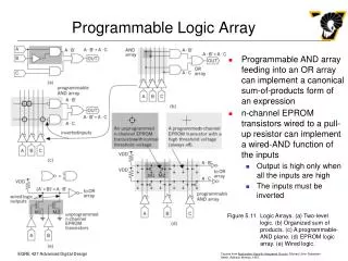
Two programmable planes • Any combination of ANDs/ORs • Sharing of AND terms across multiple ORs • Highest logic density available to user • High Fuse count, slower than PLAs • Programmable Logic Array - PLA Custom Designed Integrated Circuits
One programmable plane – AND / Fixed OR • Finite combinations of ANDs / ORs • Medium logic density available to user • Lower Fuse count, Faster than PLAs (at this time fabricated on 10 µm process • Programmable Array Logic - PAL Custom Designed Integrated Circuits
Interconnects gates Flip-Flops • Central, Global Connect • Simple, Deterministic Timing • Easily routed • PLD Tools add only interconnect • Wide, fast complex gating 50 - 200 gates Custom Designed Integrated Circuits
PLD structures PAL Macrocell LUT O1= (I1 and not I2) or (not I1 and I2) I1 I2 and or O1 =1 and Macrocell Custom Designed Integrated Circuits
36 36 36 36 Block 1Macrocell 1 to 18 Block 4Macrocell 1 to 18 Block 2Macrocell 1 to 18 Block 3Macrocell 1 to 18 18 18 18 18 I/O I/O I/O I/O PLD structures CPLD Xilinx 9572 (used in labs) I/O Blocks Switch matrix . . . . . GCK Custom Designed Integrated Circuits
PLD structures FPGA Xilinx Spartan X10 (used in projects) PLD structures LUT1(16*1 bit mem) LUT = LookUpTable O1= (I1 and not I2) or (not I1 and I2) PAL MacrocellLUT 16 product terms /LUT IO I1 LUT1 IO I2 FF1 IO O1 LUT2 IO Programmable LUTs and programmable routing Custom Designed Integrated Circuits
Interconnects Gates • Channel Based Routing • Post Layout Timin • Tools more complex than CPLDs • Fine grained • Fast register pipelining Custom Designed Integrated Circuits
ASIC/FPGA NRE NRE=Non Recurring Cost(mask cost)Non recurring=engångs 20 000kkr ASIC 10 000kkr 1000kkr FPGA 250kkr process 0,6m 0,35m 0,25m 0,13m 0,09m 0,045m Custom Designed Integrated Circuits