Advanced Alumina Transfer System for Silicon Nanowire Fabrication
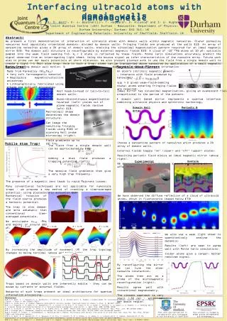
This research presents a novel Alumina Transfer System (ATS) designed to enhance the fabrication of Silicon Nanowires (SiNWs) by addressing challenges in the transfer of anodic aluminum oxide templates. Current methods face difficulties in maintaining template integrity during transfer operations, which affects the final product quality. Our ATS aims to enable the seamless transition of the template between buffer and acetone solutions, ensuring efficient PMMA-free deposition on silicon wafers. This innovative system utilizes magnetic control for precise movement and promises improvements in deposition accuracy and speed.

Advanced Alumina Transfer System for Silicon Nanowire Fabrication
E N D
Presentation Transcript
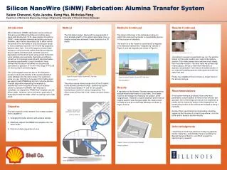
Silicon NanoWire (SiNW) Fabrication: Alumina Transfer System Salem Cherenet, Kyle Jacobs, Keng Hsu, Nicholas FangDepartment of Mechanical Engineering, College of Engineering, University of Illinois at Urbana-Champaign Introduction Silicon Nanowire (SiNWs) fabrication can be achieved through several different techniques including vapor-liquid-solid mechanism (VLS), deep reactive ion etching (DRIE), metal-assisted chemical wet etching and more. However, each method separately fails to either restrict the growth of the nanowires in only one direction (axial) or have a diameter less than 100 nm with big separation between each ‘hole’. One of the ways to resolve these issues are using a process called chemical wet etching where metallic chromium/gold nanodots were first deposited onto the silicon wafer using anodic aluminium oxide template and eventually chemical wet etching is carried out in a hydrogen peroxide and deionized water. In previous experiments, using this method, it was showed that the silicon nanowires can be precisely controlled to a precision of 10 nm in the range of 40 to 80 nm that is uniform and well aligned. One of the biggest issues we face in this fabrication process is during the transfer of the anodic aluminium oxide template onto the silicon wafer. The aluminium oxide is a very thin film so to prevent it from falling apart, we support it with PMMA and let it sit in a buffer solution. The last step before depositing the template is transferring it from the buffer solution to an acetone solution to remove the PMMA. After this step is completed, we deposit the “PMMA free” template onto the silicon wafer. However, we do not have a good way of executing the last two steps, which is causing in poor final result. Method The first step is design. Having all the requirements in mind a simple sketch of the system was made. Once a simple concept was achieved, it was translated to a 3D sketch. The picture above shows a snap shot of the 3D sketch of the alumina (aluminum oxide) transferring system. The two tubes labeled ‘’A” and “B” are used for transferring a solution in and out respectively. The silicon wafer will be hold in the I–beam structure shown below. Methods Continued The cubes at the base of the rectangle are there to restrict the motion of the I-beam in a predictable manner for the purpose of simplicity. The motion is of the I-beam is controlled by a magnetic force attraction between the ‘’magnetic tip” (shown in Figure 3) and the magnetic bar shown in Figure 4. Results A simulation of the Alumina Transfer system was made to analyze what kind of motion it could have. The I-beam moved in the straight line following the position of the ‘magnetic bar.’ However, in some situations where the bar magnet position was changed rapidly the I-beam could not keep up and as a result falls sideways as shown in Figure 5 below. Results Continued According to several of experiments we run, the alumina floated on the buffer solution but it sank in the acetone solution. This makes sense since acetone is less dense than the buffer solution. The other result we got was that it takes about a minute to have more than 90% of acetone concentration if we remove the buffer solution in our cube while adding acetone at the same time with the same flow rate. Finally, the instability of the I-rod was no longer there on the actual prototype. A I-beam B Magnetic Bar Figure 1: Alumina Transfer System-ATS Top view Photo by Salem C Figure 4: Alumina Transfer System-ATS Side View Photo by Salem C Recommendations If this system works as predicted, then some more parameters could be added to make it more efficient and accurate. One of the things one can do isto implement a robotic arm to control the motion of the magnetic bar by tracking the position of the alumina film instead of doing it manually. Another thing I recommend is incorporating a tracking system for the film since it is hard to see where it is in the buffer and/or acetone solution visually. Objective The main purpose of this research is to create a system that is capable of: Changing the buffer solution with acetone solution Effectively deposit the PMMA free template onto the silicon wafer Perform multiple deposition at once Figure 2: Structure for carrying the silicon wafer. Photo by Salem C. Acknowledgments I would like to thank Kyle Jacobs for being my graduate mentor, Keng Hsu, and Nicholas Fang for advising me. Special thanks to Shell Co. and ISUR program for sponsoring my research. Figure 5: I-beam on its side during simulation Photo by Salem C Shell Co. Magnetic tip Figure 3: Magnetic Tip for motion control Photo by Salem C