나노 기술
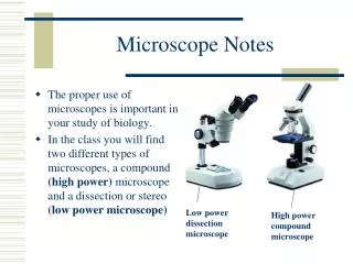
나노 기술. 기능성 산화물 박막 기술 Scanning Probe Microscope. 2002년 5월 23일 송태권. 참고 자료. 나노연구소 http://designwith.net/nano/?t=home Handbook of Nanostructured Materials and Nanotechnology. Nano?. Macro vs . Micro. Nano vs . Micro. Two ways in Nanotech. New function in nano-scale Not just size

나노 기술
E N D
Presentation Transcript
나노 기술 기능성 산화물 박막 기술 Scanning Probe Microscope 2002년 5월 23일 송태권
참고 자료 • 나노연구소 http://designwith.net/nano/?t=home • Handbook of Nanostructured Materials and Nanotechnology
Nano? Macro vs. Micro
Two ways in Nanotech. • New function in nano-scale Not just size • Bottom-up • Nanotube, Semiconductor Quantum Dots • Top-down • Nanoparticles, Nano-sized powders
Perovskites Ferroelectric Optical Magnetic Conductive High TC Superconductive Transition Metal Oxides ; Multi-valence
Ferroelectric • Ti, Zr, Nb, Ta Oxides • BaTiO3, Pb(Zr,Ti)O3, Bi4Ti3O12, La-Bi4Ti3O12, SrBi2Ta2O9 • DRAM • FRAM(Ferroelectric RAM) • IR detector
DRAM Application • High Density → Small Area → Complex Structure → High e
Optical • Nb, Ta Oxides • LiNbO3, LiTaO3 • SAW (Surface Acoustic Wave) • Non-linear Optics • Optoelectronics
Magnetic • Mn, Co, Fe Oxides • (La,Sr)MnO3 • Magnetic Head (CMR) • Magnetic Memory (MRAM) • Spintronics
Conductive • Cu, Co, Ti Oxides • (La,Sr)CoO3 • Interconnect
HTSC(High TC Superconductive) • Cu Oxides • YBa2Cu3O7-d • Joshephson Junction • SQUID • Bolometer
Detailed Topics Oxygen Vacancy Reduction Multifunctional Devices Oxygen Vacancy Reduction Multilayer Films Oxide Superlattices High Density Devices Nano-Technology Strain Control
Schematic of a FIOH Transparent Electrode (ITO) Pyroelectric (BSN, PLZT) Ferroelectric (BT, PZT) CMR Material (LSMO, LCMO) Oxide Substrate Photon; hn Monolithic Oxide Integrated Circuit Light hn Pyroelectric DP (DT) Ferroelectric DP (DT) CMR Material DR Data Storage Retrieving Data Signal Sensing & Transformation
GMR vs. CMR • Giant Magneto-Resistance • in Magnetic Metal Multilayers(Superlattices) • Colossal Magneto-Resistance • in Magnetic Oxides
Thin Film Deposition • PVD (Physical Vapor Deposition) • PLD (Pulsed Laser Deposition) • Sputtering • CVD (Chemical Vapor Deposition) • MOCVD • Sol-gel
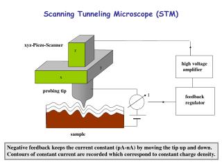
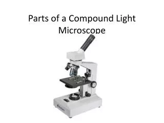
Scanning Probe Microscope • STM (Scanning Tunneling Microscope)
AFM (Atomic Force Microscope) • Non-conductive Materials like Dielectrics • In Air → Easy to Use
SCM (~ Capacitance ~) • Resonance Frequency
Applications of SCM - I • Semiconductor MOSFET
Applications of SCM - II • Memory Application