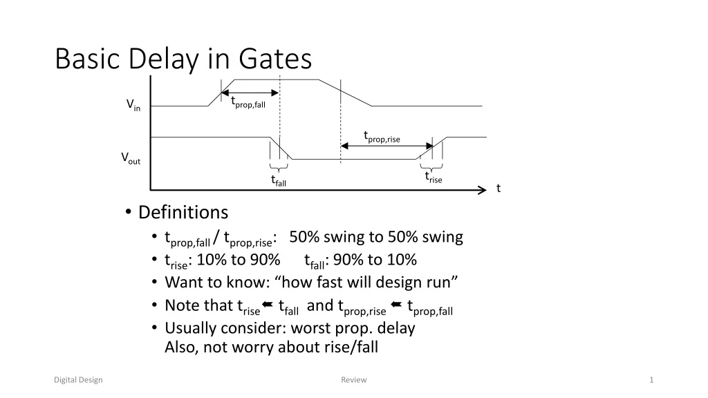

Basic Delay in Gates
E N D
Presentation Transcript
Basic Delay in Gates tprop,fall Vin • Definitions • tprop,fall / tprop,rise: 50% swing to 50% swing • trise: 10% to 90% tfall: 90% to 10% • Want to know: “how fast will design run” • Note that trise tfall and tprop,rise tprop,fall • Usually consider: worst prop. delayAlso, not worry about rise/fall tprop,rise Vout trise tfall t Review
C D E C F Q A B Critical Path Analysis “How fast will this run?” • If we change input, how long beforeoutput has correct result? • Example: responds to A much faster than D • Want to know longest time or critical path • Not all gates equal: add up delaydifferent gates / different technologies Critical path Review
Input “glitches” A • Which happens? • Depends: • Technology • How narrow pulse is relative to tprop, trise, tfall could be t B F ? or Review
A B B A F C C F Glitches (Transients) • Consider: • What is the output? • For static inputs: F=AA’=0 • Single rising edge on A • Pulse generator? • Point: Inputs to comb. logic change Transient period outputs fluctuate before final stable value Review
Hazards/False Outputs • Definition • Output takes on a value that is not predicted by the Boolean expression for either old or new inputs • Dealing with Hazards • Circuits where only a single input changes at a time • Include redundant terms (in k-map) • Can eliminate hazards • Synchronous design • Signals only sampled on clock • Period made long enough to be past transients Review
Variations in Gate Delays • Gate delay variation due to • Temperature • Vcc changes (imperfect power supply) • Process variations • Loading of gate vs. fast slow Review
4. Sequential Circuits Review
Complex Algorithms • Require • Series of operations to be performed • Order, timing important • Storage for intermediate results • Means we have memory • Digital Memory Elements • Latches • Flip-flops • SRAM, DRAM Review
R Q Q’ S SR Latch • Memory requires feedback • Circuit has two stable states • Can control with R/S inputs Review
0 R Q 0 Q’ S SR Latch • To see stability... • Can repeat for Q=1 and Q’=0. Same thing. 0 1 0 1 Review
0 0 R 1 0 Q 1 0 0 1 1 0 Q’ 0 0 S SR Latch • “Set” Operation. 1 0 1 0 1 Review
0 0 R 0 1 Q 1 0 1 0 1 0 Q’ 0 0 S SR Latch 1 • “Reset” Operation. 0 1 0 1 Review
R Q Q’ S SR Latch • Transition Table R Q S Q’ Review
SR Latch Summary • Features • Provides 1 bit of memory • Control by temporarily raising S or R • Problems? • Output can change at any time when S/R changeThink about glitches! • Inconvenient to have two inputs to controlHow do we store just the bit on a line? Review
Gated Latch R • Circuit responds when Gate=1 • Sometimes called a “transparent latch” or a “lodable latch” R Q R Q S Q’ S Q’ G S Gate Review
D-Latch D • Stores value on input D when G is high • Keeps old value otherwise • Now we can store a value, just when we want R Q D Q S Q’ Q’ G Gate Review
F D Q G Gate Using Latches • Any problems? • Level sensitive • Consider “toggle” circuitOutput: 10 or 10 each time we assert Gate • Will this work? Review
F D Q G Gate Toggle Circuit Timing • Circuit oscillates Bad • Feedback with gated latch is difficult Gate D F Review
Master/Slave Flip Flops • Idea • Use two latches to get “edge” sensitive behavior Master Slave Q1 D Q D Q D Q G G clk D Q Edge sensitive latch called a “flip flop” clk Review
0 0 0 Master Slave Q1 D Q D Q 1 D Q 0 1 G G clk Flip Flop Operation (1) • When clk=1, only first latch is transparent • Transitions on D only go through first latch! 1 1 0 0 Review
0 0 0 Master Slave Q1 D Q D Q 1 D Q 0 1 G G clk Flip Flop Operation (2) 1 • Consider storing a 1 in the flip flop • The bit got stored and sent to the output on a falling edge of clk (1=>0) • Kind of like an “airlock” • Make rising edge device with another inverter 1 1 0 1 0 Review
F D Q clk Utility of Flip Flops Example toggle circuit: Q D only on 01 transition of clk Oscillation does not occur Can store 1 bit, sampled at an edge Review
clk tsetup thold D Q tclk-q Flip Flop Timing (a) tclk-a Time until new latched value appears at output (b) tsetup Time before clock that D must be stable (c) thold Time after clock that D must be stable Review
Flip Flop Timing: tclk-q D Q • (a) tclk-q : Time for new output to appear on Q • Gate gets to slave, value propagates through Q’ Extra inverter makes + edge sensitive. clk Review
Flip Flop Timing: tsetup D Q • (b) tsetup: Time D must be stable before clock • Slave becomes transparent. Correct value must be at input! • Time to go through master stage. Q’ clk Review
Flip Flop Timing: thold D Q • (c) thold: Time D must be stable after clock • Master latches. Should be value there at clock. • Time to lower gate on master. Q’ clk Review
Registers • Definition • Storage element • One or more flip flops • Example • Four D flip flops in parallel: 4 4 D Q clk Review
D D Q Q clk EN CLK Types of Registers (1) • Loadable Register • Standard flip flop (or register)loads on every clock • May want to selectively load input • One idea: • Problems? • Adds delay to clock“clock skew” • What about glitches? Review
D Q 0 EN D 1 D Q EN CLK Types of Registers (2) • Loadable Register • Better way Review
Q3 Q2 Q1 Q0 Sin D Q D Q D Q D Q CLK Types of Registers (3) • Shift Register • Uses? • Extensions: Enable, Direction, Parallel Load, Clear, ... Review
+1 D Q CLK Counters • Implementation • Synchronous circuitmade from a register • Steps up or down on each clock edge • Input (next value) computed from output (current value) • +1 block from half adders Review
Input Forming Logic D Q Next State Comb. Logic State Memory(register) Synchronous Circuits • General synchronous circuit • Counter • State Machine Current State Review
Synchronous Circuit Design • Designing a General Counter • State transition tableCurrent state Next state • Boolean eq. fornext_state = F(curr_state) • Place flip flops between D Q F NS CS Review
Input Forming Logic Output Forming Logic D Q Outputs Next State Current State Inputs For Mealy Outputs Generalization of Sync. Circuit • Finite State Machine (FSM) • Can be used to realize general sequential algorithms • Moore outputs (depend only on state) • Mealy outputs (depend on state and inputs) Review
Input Forming Logic Output Forming Logic D Q Generalization of Sync. Circuit • Finite State Machine (FSM) Outputs Next State Current State Inputs For Mealy Outputs Review
Input Forming Logic Output Forming Logic D Q FSM Design • Process Similar to Counter • Write state transition tableImplement using comb. logic • Write truth-table or Boolean eq. for output logic • Insert registers Outputs Next State Current State Inputs For Mealy Outputs Review
00 01 10 11 State Graphs • Graphical representation of a state transition table • Helps you visualize FSM operation Value in state register CurrentState NextState Review
Inputs • Represented withlabels (signal name) onarc • Means if sig=1, takethe path (arc) clr inc’ 00 inc inc clr inc’ clr inc’ 01 11 clr inc inc 10 inc’ Review
Proper State Graphs • Conflict-free State Graph • Only one possible next statefor all possible inputs • Is previous counter with inputs conflict free? • Solve by introducing priority. • Complete State Graph • All next states are specified. • “Incomplete” means we haveomitted some cases inc 10 11 What happens when inc=‘0’ in 10? Review
00 TERM 01 11 A / MID 10 Outputs • Put names of assertedsignals next to (or in) statebubbles Means MID=1 in state 01 when A is asserted “Mealy output” Means signal TERM=1 in state 11 (0 otherwise) “Moore output” Review
Xin Seq.Rec. clk Example • Sequence recognizer “011” (Moore) Xin S0 X’in Xin X’in Z S1 X’in Z S3 X’in Xin Xin S2 Review
Xin Seq.Rec. clk Example • Sequence recognizer “011” (Mealy) Xin S0 X’in Xin/Z Z S1 X’in X’in Xin S2 Review
One-Hot State Machines • Definition • More than one state, multiple flip flops for state • “One hot” means only one flip flop active(stores a 1) at a time • Uses? • Simpler to design by handFinding next state logic tedious for very many states • Can eliminate output glitches Review
One Hot Example go’ State transition table A go stop / Y run’ stop’ B D X run C Review
A A go’ go D D D D Q Q Q Q B D stop run’ B run C Y D stop’ stop One Hot Example A State transition table B X C D Ans = Acs go’ + Dcs stop Cns = Bcs run Dns = Ccs + Dcs stop’ Bns = Acs go + Bcs run’ Review
A A go go’ D D D D Q Q Q Q B D run’ stop B run C Y D stop’ stop One Hot Example A • Glitches? • Mealy output Y Can have glitch • Moore outputFF does single trans.from CS to NSNo glitch B X C D Y Review
Summary • Number Systems / Binary Encoding • Boolean Algebra • Combinational Circuits • Sequential Circuits Fundamental concepts and terms we need for the rest of the course. Review