WP microelectronics and interconnections
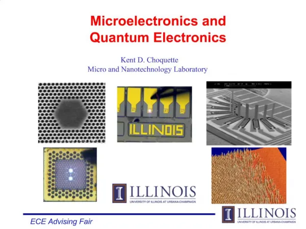
WP microelectronics and interconnections. Goal : provide chips and interconnections to the other WPs Task 1 : 65 nm chips for trackers ( CERN?) Fine pitch, low power, advanced digital processing Taks 2 : SiGe 180nm for calorimeters / gaseous (IN2p3)

WP microelectronics and interconnections
E N D
Presentation Transcript
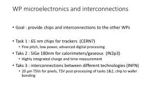
WP microelectronics and interconnections • Goal : provide chips and interconnections to the otherWPs • Task 1 : 65 nm chips for trackers (CERN?) • Fine pitch, low power, advanced digital processing • Taks 2 : SiGe 180nm for calorimeters/gaseous (IN2p3) • Highlyintegrated charge and time measurement • Taks 3 : interconnections betweendifferent technologies (INFN) • 20 µm TSVs for pixels, TSV post-processing of tasks 1&2, chip to wafer bonding
The goal of the workpackageis to provide innovative readout chips for the detectors in the otherworkpackages. Itwouldthereforeselect a fewtechnologies and providerunsboth for R&D designsthatadvance the state of the art (in speed, lownoise, integration...) and also include more mature chips that can be used to advance the detector designs and in particularallow "smart detectors" or highlyintegrated detectors. Thislatter goal alsoincludes the interconnectionaspects, againboth in R&D and applied to detectors. Itisthus split into 3 taskswhichprovidedeliverables.
Task 1 : micro electronics for trackers. • The community isfocusing a large fraction of the design work on the 65nm CMOS technology. • Presently, thismostlyaddressesmixed-signalintegratedcircuits for pixel detector readout, butitislikely to extend to more diverse applications. • For CMOS sensors, purelydigital chips (or with a dedicatedanalogsection) may be needed for the readout of a pixel matrix. • Takingadvantage of the growing expertise in 65 nm CMOS, detectors otherthansiliconones are alsointerested in usingthistechnology for new chips. • The Task willoffer 1 or 2 runs in 65 nm, where design know-how and common circuitblocks can be shared in different chips in a collaborative way by the community of IC designers.
Task 2 : micro electronics for calorimeters and gaseous detectors. • The Task willprovide 1 or 2 runs in large dynamicrange, lowpower, high speedtechnology, suchasSiGe 180nm or SOI 130nm. • The circuitswillprovide multi-channelreadout of charge and time to the accuracyrequired by these detectors. in particular, the timing properties to the fewtenpicosecondslevelwill be explored.
Task 3 : interconnections • for Task 1 and Task 2, addressing 20um TSVs for pixel sensors and interconnectionsbetweendifferenttechnologies (analog/digital or sensor/chip). • Thereis a strong interest for achieving a high-density, reliable and cost-effectiveinterconnectionbetween a readout chip and a sensor, and/or betweenanalog and digitalelectroniclayers. • ThisTask will work with industrial partners to qualifyinterconnectionprocesses with high-density 3D integrationfeaturessuchas small-pitchTSVs and wafer-to-wafer or chip-to-wafer bondingpads. 3D processeswill be selected on the basis of specificationsthat serve the community needsat best. • The Task willalsoorganize TSV post-processing and other 3D-related technologicalsteps on the CMOS wafersthatwill be fabricated in the common runs by Task 1 and Task 2. In this way, chips for diverse applicationsmayhaveaccess to wafer-level 3D technology in a prototyping stage.
WP partners • Weneedonegroup for organizing the MPWs and paying for the runs, could be CERN for Task 1, IN2P3 for Task 2 and INFN for Task 3. • Then, the runs are open for participants, wehoweverhave to find a way to limit the number of fuzzydesigns, either by requesting a financialparticipation or by selectingat the entrance the partners. • In the preparation stage of the AIDA-2 proposal, wewillask the community to submitprojects for joining the threeTasks. Projectswill be admitted to thisWorkpackage on the basis of theirscientificmerit (according to the needs of the community) and of theirfinancialcontribution to the Workpackage. • A projectmaypayitsfraction of the costs for a 65 nm prototyperun, and ask for support for TSV processing in the wafers.