Download
1 / 21
260 likes | 596 Vues
Progress Update. Modeling and Design of STT-MRAMs. Richard Dorrance Advisor: Prof. Dejan Marković July 29, 2011. “The Mighty Tyrannosaurus Rex”. Outline. Introduction Magnetic Tunnel Junction (MTJ) Modeling MTJ Characteristics STT-MRAM Memory Architectures Design-Space Analysis

E N D
Progress Update Modeling and Design of STT-MRAMs Richard DorranceAdvisor: Prof. Dejan Marković July 29, 2011
Outline • Introduction • Magnetic Tunnel Junction (MTJ) • Modeling MTJ Characteristics • STT-MRAM Memory Architectures • Design-Space Analysis • Chip Design and Results • Conclusion
Introduction • Consists of 3 basic layers • Two resistive states: • RP: Low Resistance • RAP: High Resistance • CMOS Compatible
Spintronic Operation • Spin Injector/Polarizer: • Ferromagnetic layer spin-polarize a current • Spin Detector: • Ferromagnetic layers tend to scatter anti-parallel currents
MTJ Model • Landau-Lifshitz-Gilbert equation (LLGE) based • 13 device-specific parameters: • 4 geometric, 8 material-dependent,1 empirically-derived
Cell Architectures • 1T-1MTJ • Multiple MTJs per cell Conventional Reversed Shared Stacked
Analysis of Shared Architecture • Published: • H. Park, R. Dorrance, A. Amin, F. Ren, D. Marković, C.-K.K. Yang, "Analysis of STT-RAM Cell Design with Multiple MJTs Per Access," in Proc. ACM/IEEE Int. Symp. on Nanoscale Arch. (NANOARCH'11), pp. 32-36, June 2011.
Design Space Analysis • Published: • R. Dorrance, F. Ren, Y. Toriyama, A. Amin, C.-K.K. Yang, D. Marković, "Scalability and Design-Space Analysis of a 1T-1MTJ Memory Cell," in Proc. ACM/IEEE Int. Symp. on Nanoscale Arch. (NANOARCH'11), pp. 53-58, June 2011.
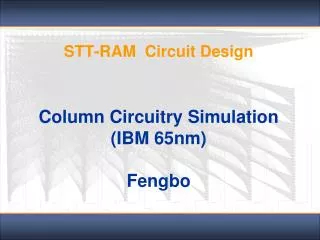
Chip Design • NO MTJ/CMOS INTEGRATION! • Designed 3 chips: • 90nm IBM bulk-CMOS (Tested) • 65nm IBM bulk-CMOS (Testing) • 45nm IBM SOI-CMOS (Waiting)
90nm Test Results • Measured Write Current: • ~300μA: 10-20ns write time • Measured Read Delay: Time to read RP (“0”) Time to read RAP (“1”)
65nm Test Results • 18-bit LFSR to digitallymeasure the read delay • Preliminary Measurements: • 500ps to 1.2ns
STT-MRAM Chip Comparison Measured TMR dependant
References • C.J. Lin, et al., "45nm low power CMOS logic compatible embedded STT MRAM utilizing a reverse-connection 1T/1MTJ cell," Electron Devices Meeting (IEDM), 2009 IEEE International , vol., no., pp.1-4, 7-9 Dec. 2009 • R. Nebashi, et al., "A 90nm 12ns 32Mb 2T1MTJ MRAM," Solid-State Circuits Conference - Digest of Technical Papers, 2009. ISSCC 2009. IEEE International , vol., no., pp.462-463,463a, 8-12 Feb. 2009 • D. Halupka, et al., "Negative-resistance read and write schemes for STT-MRAM in 0.13µm CMOS," Solid-State Circuits Conference Digest of Technical Papers (ISSCC), 2010 IEEE International , vol., no., pp.256-257, 7-11 Feb. 2010 • K. Tsuchida, et al., "A 64Mb MRAM with clamped-reference and adequate-reference schemes," Solid-State Circuits Conference Digest of Technical Papers (ISSCC), 2010 IEEE International , vol., no., pp.258-259, 7-11 Feb. 2010