Download
1 / 23
240 likes | 366 Vues
This document presents the latest advancements in DEPFET (Depleted Field Effect Transistor) pixel sensor technology as discussed at the ECFA/DESY Linear Collider Workshop in April 2003. We cover the operational principles, prototype performance, simulation results, product development status, and details about readout electronics. Innovations in design, such as thin detector areas and optimized readout architectures, allow for enhanced noise performance and low power consumption. The findings illustrate the potential for DEPFET technology in biomedical imaging and particle physics applications.

E N D
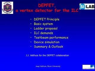
DEPFET pixel sensor – concept and status R.H. Richtera, L. Andriceka, P. Fischerb, G. Lutza, I. Pericc, J. Treisa, M. Trimplc, N. Wermesc aMPI Halbleiterlabor Munich bUniv. of Mannheim cUniv. of Bonn • DEP(leted)F(ield)E(ffect)T(ransistor) operation principles • DEPFET prototype run • Simulation and design examples • Production status • Read out electronics and steering chips • Summary R. H. Richter et al - ECFA/DESY Linear Collider Workshop, Amsterdam, 1 - 4 April 2003
Radiation ~1mm - - - + - + - + + - DEPFET-Principle ~300 mm FET integrated on high ohmic n-bulk Collection of electrons within the internal gate Modulation of the FET current by the signal charge! Advantages: Amplification of the charge at the position of collection => no transfer loss Full bulk sensitivity Non structured thin entrance window (backside) Very low input capacitance => very low noise R. H. Richter et al - ECFA/DESY Linear Collider Workshop, Amsterdam, 1 - 4 April 2003
Proposed concept for TESLA matrix is read out row-wise first thinned samples: • thin detector-area • down to 50µm • frame for mechanical • stability carries readout- • and steering-chips [L.Andricek, MPI Munich] R. H. Richter et al - ECFA/DESY Linear Collider Workshop, Amsterdam, 1 - 4 April 2003
Excellent noise values measured on single pixels 55Fe-spectra @ 300K ENC = 4.8 +/- 0.1 e- R. H. Richter et al - ECFA/DESY Linear Collider Workshop, Amsterdam, 1 - 4 April 2003
BioScope - imaging of tracer-marked bio-medical samples (P. Klein and W. Neeser) Noise: ca. 70 ENC @ 300K Slow operation (old technology) Large arrays are impossible (JFET => VP variations) Large cell size
DEPFET pixel matrix Low power consumption Fast random access to specific array regions • Read filled cells of a row • Clear the internal gates • of the row • - Read empty cells R. H. Richter et al - ECFA/DESY Linear Collider Workshop, Amsterdam, 1 - 4 April 2003
DEPFET Technologyon 6” wafer Double poly / double aluminum process on high ohmic n- substrate perpendicular to channel (with clear) along p-channel R. H. Richter et al - ECFA/DESY Linear Collider Workshop, Amsterdam, 1 - 4 April 2003
Rectangular DEPFET pixel detector MOS transistor instead of JFET A pixel size of ca. 20 x 20 µm² is achievable using 3µm minimum feature size. R. H. Richter et al - ECFA/DESY Linear Collider Workshop, Amsterdam, 1 - 4 April 2003
Active Pixel Sensor (rectangular) • 2 pixels • 30 x 30 µm² • DEPFET • L = 5 µm • W = 18 µm • reduce the required read out speed by 2 doubles the number of read out channels
Depth 10µm Depth 7µm Depth 4µm Depth 1µm External (internal) Gates Sources n+ clear contacts Drain Cell size 36 x 27 µm² Potential during collection - 3D Poisson equation (Poseidon) (50µm thick Si, NB=1013cm-3,VBack=-20V) R. H. Richter et al - ECFA/DESY Linear Collider Workshop, Amsterdam, 1 - 4 April 2003
Current production statusPixel array section – design with clockable clear gate 1 pixel cell • Done: • N-side with two polysilicon layers and contact openings • Backside processing • Aluminium Sputtering • To do: • 1st metal lithography (2 weeks) • First measurements • 2nd metal process Drain Gate Clear Clear gate Source R. H. Richter et al - ECFA/DESY Linear Collider Workshop, Amsterdam, 1 - 4 April 2003
Readout architecture (triggerless) • FIFO is emptied row wise: • hit identification with current comparator and store hit pattern in FIFO (digital part) DEPFET provides current + fast readout needed Þ current based readout (see Vertex2002 proceedings) • keep potential at input node constant (regulated cascode) • (signal+pedestal current) stored in current memory cell (inverting property) • pedestal current after reset subtracted automatically • signal value is stored in FIFO (analog part) • ‘hit finder’ identifies hits in a row • and multiplexes (MUX) the appropriated currents to ADC • (respective analogous outputs) R. H. Richter et al - ECFA/DESY Linear Collider Workshop, Amsterdam, 1 - 4 April 2003
Chip development for TESLA Readout chip 1.0: Steering chip: • TSMC 0.25µm, 5metal • radiation tolerant design with annular nmos transistors • contains: various current memory cells, hit finder, comparator • size: 4 x 1.5 mm2 [I.Peric (Bonn) / P.Fischer (Mannheim)] • AMS 0.8µm HV-Process • steers 64 DEPFET-rows (cascadable) • size: 4.6 x 4.8 mm2 • internal sequencer flexible pattern [M.Trimpl (Bonn)] R. H. Richter et al - ECFA/DESY Linear Collider Workshop, Amsterdam, 1 - 4 April 2003
I2U U2I Results steering chip: works with 50MHz @ 15pF load capacitance R/O chip: • digital part: • hitfinder und comparator work with 50MHz • analoge performance: • 25 MHz sample frequency • 0.1 % differential nonlinearity • (for 10µA (~ 10000 e-) dyn. input range) • 38 e- Noise (for complete analogous stage) [Testsetup for current memory cells] Þ Readout concept works R. H. Richter et al - ECFA/DESY Linear Collider Workshop, Amsterdam, 1 - 4 April 2003
Prototype system ... • R/O chip (July 2003): • readout chip with 128 channels • 50MHz sample frequency • 25 e-noise Hybrid r r e e h h c c t t i i w w DEPFET -Matrix S S - - (25x25 µm) t e e t s a e G R • Hybrid-PCB with • separate steering chips für select und reset • 64x128 pixel array • new R/O-Chip • Readout-PCB with • ADC and RAM (external) • Datatransfer between Hybrid and PC R/O Chip 2.0 Readout-PCB Sequencer ADC PC DATA-RAM Controller R. H. Richter et al - ECFA/DESY Linear Collider Workshop, Amsterdam, 1 - 4 April 2003
Summary / schedule • Key features: low noise, full bulk sensitivity, no charge transfer loss, low power consumption, random access within an array • A new DEPFET technology (2 poly/ 2 aluminum) was developed for large arrays and high speed operation. • A DEPFET prototype production has been started with DEPFET arrays • 30 x 30 µm² pixel size. • First measurements in 2 weeks • Read out electronics first test chip successfully tested (50MHz operation possible) • 128 channel read out chip (2.0) currently in design, submission this month, chip delivery in summer • Steering chip for Gate and Clear access successfully fabricated • (first tests very encouraging) • Complete prototype system ready by end of the year • Further plans • In 2004: Design and production of large arrays • Some wafer on SOI (thinned technology) ? R. H. Richter et al - ECFA/DESY Linear Collider Workshop, Amsterdam, 1 - 4 April 2003
Back up transparencies R. H. Richter et al - ECFA/DESY Linear Collider Workshop, Amsterdam, 1 - 4 April 2003
Crossing polysilicon lines Problems with demolished polysilicon lines and bad polyI/polyII insulation Solved now R. H. Richter et al - ECFA/DESY Linear Collider Workshop, Amsterdam, 1 - 4 April 2003
Self aligning Technology Positions of all essential implantations are determined not by masks but by polysilicon layers shallow channel implantation • mandatory for rectangular cells • (lateral channel definition) • - reduces parameter variations • on the wafer R. H. Richter et al - ECFA/DESY Linear Collider Workshop, Amsterdam, 1 - 4 April 2003
Depth 1µm Hiding the n+-clear contacts The positive Clear pulse removes the electrons from the Internal Gate and also pushs the holes out of the deep p cover region. After returning of the clear the deep p remains negatively charges forming a shield for the signal electrons. R. H. Richter et al - ECFA/DESY Linear Collider Workshop, Amsterdam, 1 - 4 April 2003
Poseidon (3D Poisson equ.) Includes 3D effects => VClear=20V Simulation of the Clear mechanism TeSCA (2D, time dependent) Removal of 1600 electrons from the internal gate (VClear=15V)
Pixel prototype production (6“ wafer)for XEUS and LC (TESLA) Aim: Select design options for an optimized array operation (no charge loss, high gain, low noise, good clear operation) On base of these results => production of full size sensors Many test arrays - Circular and linear DEPFETS up to 128 x 128 pixels minimum pixel size about 30 x 30 µm² - variety of special test structures Production will be finished in spring R. H. Richter et al - ECFA/DESY Linear Collider Workshop, Amsterdam, 1 - 4 April 2003
imaging spectroscopy 7.68 x 7.68 cm² 1024 x 1024 pixels 1 Mpix 75 µm 300 ... 500 µm 4 el. ENC 1.2 msec 2.5 µsec purpose detector format pixel size thickness noise readout time / detector / row particle tracking 1.3 x 10 cm² (x 8) 520 x 4000 pixels (x 8) 2.1 Mpix (x8) 25 µm 50 µm ~ 100 el. ENC 50 µsec 20 nsec