Main control
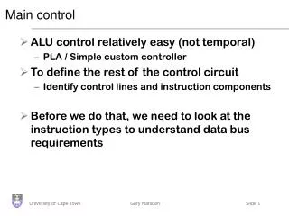
Main control. ALU control relatively easy (not temporal) PLA / Simple custom controller To define the rest of the control circuit Identify control lines and instruction components Before we do that, we need to look at the instruction types to understand data bus requirements.

Main control
E N D
Presentation Transcript
Main control • ALU control relatively easy (not temporal) • PLA / Simple custom controller • To define the rest of the control circuit • Identify control lines and instruction components • Before we do that, we need to look at the instruction types to understand data bus requirements
Instruction analysis Target register* Base register 31-26 25-21 20-16 15-11 10-6 5-0 R op rs rt rd shamt funct LS op rs rt address B op rs rt address offset * This implies a Mux
What do the orange bits do? • RegDest • Source of the destination register for the operation • RegWrite • Enables writing a register in the register file • ALUsrc • Source of second ALU operand, can be a register or part of the instruction • PCsrc • Source of the PC (increment [PC + 4] or branch) • MemRead / MemWrite • Reading / Writing from memory • MemtoReg • Source of write register contents
Building the control unit • All but one of the 7 lines can be set using op-code bits • PCSrc is determined by output from the ALU as well as op-code (need an AND gate) • Besides this 7, there are 2 for the ALUOp • To set these, all we need are the 6 bits determining the op-code
Sample R-type execution • Instruction fetched and PC incremented • $2 and $3 are read from register file • ALU operates on the data • The result from the ALU is written to register file
Finalising control • Actual Op code
Limitations of single cycle • Clock cycle identical for every instruction • CPI = 1 • Bound by longest instruction (load word) • Inst., register, ALU, data memory, register • Not all instructions will take this long • Memory access: 8 ns • Register access: 2 ns • ALU: 4 ns
Comparative timing • No very efficient!
Multicycle implementation • Previously, instruction broken in to a series of steps corresponding to the functional unit operations need • Can use these steps to create a multi-cycle implementation where each step is the execution takes one clock cycle • Unit can be used more than once (on different cycles) • Can help reduce the total amount of hardware required • Trade-off with complex control
Differences • Single instruction / data memory • Single ALU • Some extra registers for buffers (more later)
Implications • Need to add more Muxs and registers (cheap) • New control signals • Write signal for each state element (PC, memory, register file, instruction register) • Read signal for memory • ALU control unit (as before) • But we can ditch two adders and memory unit
Breaking into Clock Cycles • Examine what happens in each clock cycle of each instruction to make sure we have enough elements (e.g. registers, control lines) • Registers introduced when • Value computed in one cycle and used in another • Inputs to a block change before output can be written to a state element • Mem -> ALU -> Mem
Goal of execution cycles • Balance the amount of work done each cycle to minimize the cycle time • In our case, we use 5 steps • Each step limited to • At most one ALU op • One register access • One memory access • Clock cycle will be same as the longest of these
Instruction steps • Instruction fetch • Instruction decode and register fetch • Execution, mem address completion or branch completion • Memory access or R-type write back • Write back • Using this information we can determine what control must do in each clock cycle
Instruction fetch • Load instruction from memory • IR = Memory [PC] • Set Read address mux (IorD) = 0 select instruction • Set MemRead = 1 • Increment PC • PC = PC + 4 • Set ALUSrcA = 0 get operand from IR • Set ALUSrcB = 01 get operand '4' • Set ALUOp = 00 add • Allow storing new PC in PC register
Instruction decode and fetch • Switch registers to the output of the register block • A = register [IR [25-21]] rs • B = register [IR [20-16]] rt • No signal setting required • Calculate the branch target address target = PC + (sign-ext. (IR [15-0]) << 2) • Stored in the ALUOut register • Set ALUSrcB = 11 • Set ALUOp = 00 add
Memory access Execution • Step depends on the instruction • Selection performed by interpretation of the op + function field of the instruction • Calculate memory reference address • ALUOut = A + sign-ext. (IR[15-0]) • Set ALUSrcA = 1 get operand from A • Set ALUSrcB = 10 get operand from sign extension unit • Set ALUOp = 00 add
Execution II • Arithmetic-logical instruction (R-type) • ALUOut = A op B • Set ALUSrcA = 1 get operand from A • Set ALUSrcB = 00 get operand from B • Set ALUOp = 10 code from IR • Branch: if (A == B) PC = ALUOut • Set ALUSrcA = 1 get operand from A • Set ALUSrcB = 00 get operand from B • Set ALUOp = 01 subtraction • Write ALUOut to PC register
Mem access complete • Memory access • ALU controls must remain stable • Set I or D = 1 address from ALU • memory-data = memory [ALUOut] • load from memory • Set MemRead = 1 • memory [ALUOut] = B • store to memory • Set MemWrite = 1
R-type complete • Arithmetic-logical instruction complete • Register [IR [15-11]] = ALUOut • Set RegDst = 1 Select write register • Set RegWrite = 1 Allow write operation • Set MemToReg = 0 Select ALU data • ALUOp, ALUSrcA, ALUSrcB = constant
Write-back • Write data from memory to the register • Reg [IR[20-16]] = memory-data • Set RegDst = 0 Select write rt as target register • Set RegWrite = 1 Allow write operation • Set MemToReg = 1 Select Memory data • ALUOp, ALUSrcA, ALUSrcB = constant
Defining Control • Single cycle path • Construct a truth table and mapped them to logic gates • Multi-cycle • Tricky because of temporal aspect • Control must specify • Signal settings • Next step in execution • Two techniques • Finite State machines (usually graphically represented) • Microprogramming (code representation)
Finite State Machines • Consists of • Set of states • Rules for moving between states • Details • Each state has a set of asserted outputs • Those not explicitly asserted are de-asserted • States correspond to the 5 stages of execution • Each step takes one clock cycle • Initial two states are common
FSM Implementation • A register to hold current state • A block of combinational logic to determine: • Datapath signals to be asserted • The next state
Microprogramming • Design the control as a program that implements the machine instructions in terms of simpler microinstructions • For our subset, FSM are fine • For full instruction set (>100) which vary from 1 to 20 cycles more complexity is required (diagrams insufficient) • Use ideas from programming to create a simpler way to define control • Control instructions are referred to as microinstructions (as opposed to MIPS inst.)
More Microprogramming • Each instruction defines ‘the set of datapath control signals that must be asserted in a given state’ • ‘executing’ a microinstruction has the effect of asserting the specified control lines • Format • Symbolic representation of the control that is translated in to control logic • Can choose number of mInstruction fields and what control signals are affected by each field
Choices • Format is chosen to simplify representation • Improving programmer comprehension • A lot better than pure binary to specify how a Mux is set • Besides the format of the instruction, we need to figure out the order of execution
Choosing next MicroInstruction • Increment address of current mInstruction to get next mInstruction (Seq) - default • Branch to the mInstruction that begins execution of the next MIPS instruction (Fetch) • Choose next instruction based on control unit (Dispatch) • Implemented via a lookup (dispatch) table containing addresses of target mInstructions • Often multiple tables • Kind of like a switch statement