CD4007 CMOS Pairs
CD4007 CMOS Pairs. Electronic Design Laboratory. Overview. CD4007 Dual Complementary Pair Plus Inverter Rise Time and Fall Time Design Number Documents Six Configurations. CD4007. CD4007. Reference Inverter and Center Pair. Warnings.


CD4007 CMOS Pairs
E N D
Presentation Transcript
CD4007 CMOS Pairs Electronic Design Laboratory
Overview • CD4007 Dual Complementary Pair Plus Inverter • Rise Time and Fall Time • Design Number Documents • Six Configurations
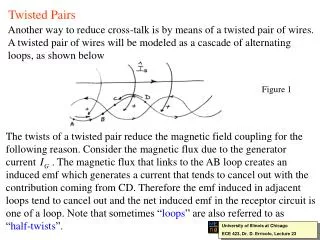
CD4007 Reference Inverter and Center Pair
Warnings • Don’t subject CD4007 to high voltages or static electricity. • Store CD4007 in an anti-static bag or in anti-static foam. • Momentarily touch a metal part of the workbench to discharge yourself before handling the part or touching the leads. • Never let voltage on any pin be more positive than pin 14 or more negative than pin 7. The circuit may “latch up”— possibly causing permanent damage.
Warnings • Always connect pin 7 (substrate for n-channel transistors) to your negative supply voltage and pin 14 (substrate for p-channel transistors) to your positive supply voltage. • Connect or turn-on the supply voltages (pins 7 & 14) before any other voltages in your circuit. • For added safety, ground any unused inputs.
Standard Load -- Pin 12 47 pF
Rise & Fall Time VOUT 100% 90% 10% 0% time Fall Rise
Rise Time VDD PLH = 1.29 RonpC r = 2 PLH r = 2.58 RonpC Ronp 47 pF VC(0) = 0 V
Fall Time VC(0) = 5 V PHL = 1.29 RonnC f = 2 PHL f = 2.58 RonnC 47 pF Ronn
2 1 5 4 14 13 8 7 11 12 9 1SP 1DP 1A 1DN 1SN VDD 2A 2DP 2DN VSS 3SP 3A 3Y 3SN 3 6 10 Design Number Document
VDD 2-Input NAND RISE and FALL Worst-Case One Pull up Ronp for RISE Worst-Case Two Pull up Ronn for Fall
Six Configurations • Inverter • Triple Inverter
Six Configurations • 3-Input NAND • 3-Input NOR
Six Configurations • OR-AND-INVERT (OAI) • OUT = (A+B)•C • 1Y = (1A+3A)•2A
Six Configurations • Dual Bi-Directional Transmission Gate