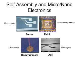
Why do we put the micro in microelectronics?
Why do we put the micro in microelectronics?. Why Micro?. Lower Energy and Resources for Fabrication Large Arrays Minimally Invasive Disposable Smaller Time Scales Lower Cost What about the Physics?. Scaling at the Microscale. Not all properties scale in the same way!. Volume Forces

Why do we put the micro in microelectronics?
E N D
Presentation Transcript
Why Micro? • Lower Energy and Resources for Fabrication • Large Arrays • Minimally Invasive • Disposable • Smaller Time Scales • Lower Cost What about the Physics?
Scaling at the Microscale Not all properties scale in the same way! Volume Forces Gravity Inertia Mass Surface Forces Surface Tension Viscosity Heat Loss
Animal Kingdom Larger Animals Limited number Limited environments Slow Gravity limited Small Animals Heat loss size2 Heat generation size3 Large energy intake (food)
Why can’t I walk on water? weight scales as l3 surface tension scales as l As animals become smaller, weight decreases more rapidly than surface tension.
Why can’t I lift a car? weight scales as l3 strength scales as l2 ants can carry 50 time their weight a human shrunk to ant size could carry 300 times his/her own weight an ant increased to human size will not be able to support it’s own weight
Example: Digital Mirrors Digital Light Processing (DPL)
Digital Light Processing: A New MEMS-Based Technology By Larry Hornbeck
Acceleration direction Support Arms Mass Anchor Anchor Displacement sensor Accelerometer: Analog Devices Inc. Commercially available two-axis accelerometer
A Polysilicon Accelerometer (2 Microns Thick) Mass Sensing Electrodes Support Arms Support arms are 2 microns square and ~ 100 microns long From John Yasaitis, Analog Devices Inc
Closeup of ADI Accelerometer From John Yasaitis, Analog Devices Inc
Many Properties Depend on Atomic Structure Silicon Crystalline Materials Regular arrangement of atoms with long range order
holes electrons Si Si Si 0.235 nm 0.543 nm Si Si Si Si Si Si Silicon Si semiconductor 5 silicon atoms in a unit cell Diamond lattice Covalent bonds 14 electrons 4 valence electrons Silicon molecules: http://www.eere.energy.gov/pv/simolecule.html
Integrated Circuits in 1958 Jack Kilbyat Texas Instruments
Integrated Circuits in 1962 RTL Logic (Noyce and Hoerni)
Integrated Circuits in 1965 Operational Amplifier, Fairchild ua 709
Integrated Circuits in 1991 Power PC, AIM (Apple-IBM-Motorola Alliance)
Today’s Microelectronics & MEMS Analog Devices, Accelerometers and Gyroscopes
Decrease in Minimum Feature Size with Time (Moore’s law)
Clean Room Classification English system: Numerical designation of the class is maximum allowable number of particles that are 0.5 mm and larger per cubic foot of air. Metric system: Numerical designation of the class is taken from the Logarithm (base 10) of the maximum allowable number of particles that are 0.5 mm and larger per cubic foot of air IC is very sensitive to particles. It usually requires Class 10 or better MEMS is more robust to particulates
Microfabrication Silicon Oxidation Photoresist Deposition Masking and Exposure Figures from May and Sze
Photoresist Development Doping Si02 etching Metallization Metallization Patterning Photoresist Cleaning Figures from May and Sze
Thermal Oxidization • Dry Oxidization : Si (solid) + O2 (gas) SiO2 (solid) • Wet Oxidization: Si (solid) + 2H2O (gas) SiO2 (solid) + 2H2 (gas)
Photolithography: Pattern Transfer The remaining image after pattern transfer can be used as a mask for subsequent process such as etching, ion implantation, and deposition.
bound electrons Si Si Si Si Si Si Si B Si Si P Si Si Si Si Si Si Si Doped Silicon P- doped N- doped free electrons holes Silicon molecules: http://www.eere.energy.gov/pv/simolecule.html
Diffusion Constant source – High surface concentrations, shallow, "deposition“ Limited source – Low surface concentrations, deep, "drive-in"
Thin Film Deposition Thermal Evaporator • Pump down to 1 mtorr • ( 1 torr = 1 mmHg) • Place wafers upside down to reduce particles • Heat sources until white hot • Low pressure = long mean-free-path (i.e., directional deposition) • Use shutter for better timing
LIGA: electroplating nickel www.me.mtu.edu/~microweb