
Self Assembly and Micro/Nano Electronics
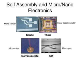
Self Assembly and Micro/Nano Electronics. Micro-accelerometer. Micro-sensor. Micro-mirror . Micro-gear. What are MEMS/NEMS?.

Self Assembly and Micro/Nano Electronics
E N D
Presentation Transcript
Self Assembly and Micro/Nano Electronics Micro-accelerometer Micro-sensor Micro-mirror Micro-gear
What are MEMS/NEMS? Micro-Electro-Mechanical Systems (MEMS) are the integration of mechanical elements, sensors, actuators, and electronics on a common silicon substrate through microfabrication technology. Micro-accelerometer Micro-sensor Micro-mirror Micro-gear
MEMS vs. Integrated Circuits (IC’s) • One way to look at it: • IC’s move and sense electrons • MEMS move and sense mass • MEMS act as transducers (sensors) converting a physical property into an electrical property (force to voltage, etc…). • MEMS can also actuate mechanical devices (switches, mirrors, etc…)
1982 LIGA Process Introduced • In the early 1980s Karlsruhe Nuclear Research Center in Germany developed LIGA • LIGA is a German acronym for X-ray lithography (X-ray Lithographie), Electroplating (Galvanoformung), and Molding (Abformung) • It allows for manufacturing of high aspect ratio microstructures • High aspect ratio structures are very skinny and tall • LIGA structures have precise dimensions and good surface roughness Microfluidic device made using LIGA process Capacitive Comb drive also made using the LIGA process
1986 Invention of the AFM • In 1986 IBM developed the atomic force microscope (AFM) • The AFM maps the surface of an atomic structure • Measures the force acting on the tip of a microscale cantilever • It is a very high resolution type of scanning probe microscope with a resolution of fractions of an Angstrom
MEMS Applications • Pressure Sensors • Auto and Bio applications • Ink Jet Print Heads • Accelerometers • (Inertial Sensors – “Crash Bags”, Navigation, Safety, iPhones) • Micromachines • Micro Fluidic Pumps • Insulin Pump (drug delivery) • Spatial Light Modulators (SLM’s) • MOEM – Micro Optical Electro Mechanical Systems • DMD – Digital Mirror Device • Mass Storage Devices • Chem Lab on a Chip • Cantilever biosensors
MEMS Pressure Sensors • Pressure Sensors • Use piezoresistive silicon sensors • The silicon chip flexes as pressure changes • The amount the silicon chip flexes determines the output voltage signal. These sensors help improve engine performance including gas mileage.
Pressure Sensors TRW Commercial Gas Engine Sensor - 1985 Top view of the TRW (1985) pressure sensor, the metal components are on top of the silicon membrane. The silicon membrane is stressed when there is a pressure differential.
Intercardial catheter-tip sensors These MEMS transducers are used in intercardial catheter-tip sensors for monitoring blood pressure during cardiac catheterization. 0.15 x 0.4 x 0.9 mm Photo courtesy of Lucas NovaSensor, Fremont, CA.
Disposable Blood Pressure Sensors Disposable sensors use MEMS transducers to measure changes in blood pressure. Photo courtesy of Motorola, Sensor Products Div., Phoenix, AZ. These $10 devices connect to a patient's IV line and monitor blood pressure through the IV solution.
EmKay Sisonic Microphone This microphone is made from Silicon and is only millimeters large.Photo Courtesy of EmKay
Ink Jet Ink jet printers are MEMS based – 1979 IBM and HP
Ink Jet Ink jet printers are MEMS based – 1979 IBM and HP
1979 HP Micromachined Inkjet Nozzle Close-up view of a commercial inkjet printer head illustrating the nozzles. Schematic of an array of inkjet nozzles. This printing technique rapidly heats ink, creating tiny bubbles. When the bubbles collapse, the ink squirts through an array of nozzles onto paper and other media. Silicon micromachining technology is used to manufacture the nozzles. The nozzles can be made very small and can be densely packed for high resolution printing.
The Accelerometer Analog Devices – 1993 Saab was the first automobile company to include MEMS accelerometers to trigger airbags. These MEMS-based systems sense rapid deceleration and in the event of a collision send a signal to inflate rapidly an airbag.
The Accelerometer An accelerometer is a sensor for testing the acceleration along a given axis. The simplest MEMS accelerometer is an inertial mass suspended by springs. Deflection of the mass is converted into an electrical signal.
iPhoneNintendo WiiIBM Thinkpad http://www.youtube.com/watch?v=VmDnuqEOLps&feature=related http://www.youtube.com/watch?v=Z24JP5TBnyE
MEMSIC's Dual-Axis Thermal Accelerator The square in the middle of the chip is a resistor that heats up a gas bubble. The next larger squares contain thermal couples that sense the location of the heated bubble as the device is tilted or accelerated. (Image courtesy of MEMSIC, Inc.)
MEMS as Machines MEMS are often referred to as Micro Machines. Tiny devices that move things. Mirror (popped up) Gear Train. Each gear tooth is 8 microns wide.
Micro Machines • Surface Micromachining takes off in the 1990’s. • Sandia National Laboratories This basically consists of alternating layers of structural materials (polycrystalline silicon) and sacrificial layers (Silicon Dioxide). The sacrificial layer is a scaffold and acts as a temporary support and spacing material. The last step of the process is the “release” step, where the sacrificial layer is removed freeing the structural layers so they can move.
Micromachines In this image, the square at the top is a microfluidics device with internal passageways used for a "lab on a chip." The multi-arm device (center) is a fuel injection nozzle. Bottom left is an accelerometer, and bottom right is an inductor used in RF circuits. (Image courtesy of Microfabrica Inc., www.microfabrica.com.)
Micromachines Microfluidics Device In this image, the square at the top is a microfluidics device with internal passageways used for a "lab on a chip." The multi-arm device (center) is a fuel injection nozzle. Bottom left is an accelerometer, and bottom right is an inductor used in RF circuits. (Image courtesy of Microfabrica Inc., www.microfabrica.com.)
Micromachines Microfluidics Device Fuel Injection Nozzle In this image, the square at the top is a microfluidics device with internal passageways used for a "lab on a chip." The multi-arm device (center) is a fuel injection nozzle. Bottom left is an accelerometer, and bottom right is an inductor used in RF circuits. (Image courtesy of Microfabrica Inc., www.microfabrica.com.)
Micromachines Microfluidics Device Fuel Injection Nozzle Accelerometer In this image, the square at the top is a microfluidics device with internal passageways used for a "lab on a chip." The multi-arm device (center) is a fuel injection nozzle. Bottom left is an accelerometer, and bottom right is an inductor used in RF circuits. (Image courtesy of Microfabrica Inc., www.microfabrica.com.)
Micromachines Microfluidics Device Fuel Injection Nozzle Accelerometer Inductor In this image, the square at the top is a microfluidics device with internal passageways used for a "lab on a chip." The multi-arm device (center) is a fuel injection nozzle. Bottom left is an accelerometer, and bottom right is an inductor used in RF circuits. (Image courtesy of Microfabrica Inc., www.microfabrica.com.)
MEMS-based Optical Switch Micro Optical Electro Mechanical Systems (MOEMS) In 1999 Lucent Technologies developed the first optical network switch • These MEMS optical switches utilize micro mirrors to switch or reflect an optical channel or signal from one location to another.
Digital Mirror Device (DMD) A DMD chip has on its surface several hundred thousand microscopic mirrors which correspond to the pixels in the image to be displayed. Digital Light Projector (DLP)
Digital Mirror Device (DMD) The mirrors can be individually rotated ±10-12°, to an on or off state.
How Small are these Mirrors? Pin Point Each mirror is about 16μm square! Ant Leg DMD mirrors – complete DLP units have over 2 million mirrors – all functioning!
Mass Storage - IBM It works by making small indentations in a polymer film. Higher density data capability IBM’s “Millipede” 100 Tera Bit per square inch!
Mass Storage - IBM • A two-dimensional array of V-shaped silicon cantilevers, each 70 µm long. • Writes divot into polymer by heating tip to 400°C • Reads by looking at surface with 300°C tip (measures resistance change with temp drop) • – if the tip is in a divot, the tip cools more than if it is not – therefore, there is a change in resistivity which is measured by the electronics. • Erases by making an offset pit, which causes the nearby pit to “pop up” and hence erases it.
Nucleus Ribosome Eukaryoticcells Bacteria Viruses Proteins 100 µm 10 µm 1 µm 0.1 µm 0.01 µm 0.001 µm (10 nm) (1 nm) Surface Micromachining Features (MEMS) Visible Light Gate of Leading Edge Transistor Molecules BioMEMS The overlap between microbiology and microsystem feature sizes makes integration between the two possible Atom
Biomedical Applications • Scientists are combining sensors and actuators with emerging biotechnology • Applications include drug delivery, DNA arrays, and microfluidics
Biomedical Applications Micromachine needles used to deliver drugs Procter and Gamble Plastic Needle Array
Cantilevers are used as Sensors Cantilevers are used as Switches Many MEMS Sensors use the principles of Cantilevers as well as RF Swtiches MEMSCantilevers
What is a Cantilever? Cantilevers have a resonant frequency that depends on the length and the mass.
MEMS Cantilever sensors • The ends of the cantilevers are coated with a layer of probe molecules. • When a target molecule is present, it attaches to the probe molecule, thereby increasing the mass. • The resonant frequency goes down. • You just detected the presence of a molecule!
Cantilever Sensors As mass is added to the cantilever shifts the resonance frequency. A gold dot, about 50 nanometers in diameter, fused to the end of a cantilevered oscillator about 4 micrometers long. A one-molecule-thick layer of a sulfur-containing chemical deposited on the gold adds a mass of about 6 attograms (10-18 grams) , which is more than enough to measure.Craighead Group/Cornell Univeristy
Resonance Shift School of Applied and Engineering Physics and the Nanobiotechnology Center, Cornell University Resonance Shift due to Single Cell 5 x 15um Cantilever with an E. Coli cell bound to antibody layer. Black is the response before cell attachment, Red is after cell attachment. http://www.news.cornell.edu/releases/April04/attograms.ws.html
Detection of Single DNA Gold dot = 40nm SiN thickness = 90nm By changing the coating (Nano) one can functionalize the cantilever to detect single strands of DNA. Mass resolution is on the order of under 1 ato gram (10-18grams) http://www.hgc.cornell.edu/Nems%20Folder/Enumeration%20of%20Single%20DNA.html