Download
1 / 1
10 likes | 132 Vues
This study presents an analysis of using a bias-free vertical-cavity surface-emitting laser (VCSEL) for optical data transmission, focusing on power consumption and bit-error rate (BER) implications. Simulation results show the impact of bias current settings on power usage and BER, along with strategies for mitigating eye diagram distortion and improving signal equalization. The findings provide insights into optimizing the performance of bias-free VCSEL transceivers for efficient high-speed data transmission.

E N D
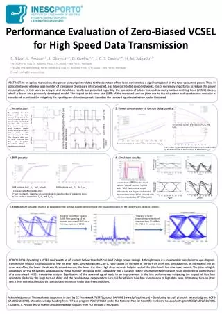
Performance Evaluation of Zero-Biased VCSEL for High Speed Data Transmission S. Silvaa, L. Pessoaa,b, J. Oliveiraa,b, D. Coelhoa,b, J. C. S. Castroa,b, H. M. Salgadoa,b aINESC Porto, Rua Dr. Roberto Frias, 378, 4200 - 465 Porto, Portugal bFaculty of Engennering, Porto University, Rua Dr. Roberto Frias, S/N, 4200 - 465 Porto, Portugal E-mail: ssilva@inescporto.pt ABSTRACT: In an optical transceiver, the power consumption related to the operation of the laser device takes a significant parcel of the total consumed power. Thus, in optical networks where a large number of transceiver devices are interconnected, e.g. large distributed sensor networks, it is of extremely importance to reduce this power consumption. In this work an analysis and simulation results are presented regarding the operation of a bias-free vertical-cavity surface-emitting laser (VCSEL) device, which is based on a previously developed model. The impact on bit-error rate (BER) of the increased turn-on jitter due to the bit-pattern and spontaneous emission is considered. A method for mitigating the eye-diagram distortion penalty based on the received signal equalization is also illustrated. 1. Introduction: 2. Power consumption vs. turn on delay penalty: By operating the laser device with no bias-current (0 current at the logic 0 stage) a significant power saving can be made regarding the optimum bias current operation mode. However a penalty in the eye diagram shape will occur and, consequently, in the BER. This is because of the turn-on delay increased jitter due to bit-pattern dependent effects and spontaneous emission. Input Current Normal Bias Turn on delay (τd) time as a function of Ion/Ith and Ioff/Ith. Carrier build up due to bit pattern effects and resulting optical output. Carrierdensity Zero Bias Opticalpower output Power consumption in the laser device as a function of Ioff/Ith. Turn on jitter (ton) probability distribution function for several ratios (η) of carrier life time to bit duration (T) as a function of ton/T. 3. BER penalty: 4. Simulation results: 850nm VCSEL Turn on delay difference due to bit pattern. ‘dashed’: current into the laser; ‘solid’: laser optical output. BER estimate for Ion/Ith , for Ioff=0 mA BER estimate for Ion/Ith , for Ioff=Ith. 1310nm VCSEL • Considering BER limited by jitter: • Turn on jitter (ton) depends on turn on delay (τd) and number of preceding zeros. • Turn on delay depends on Ion/Ith and Ioff=Ith. Although the eye diagram is distorted, data transmission could be achieved with a bit error rate bellow 10-9 (50ps jitter). Bias No bias 5. Equalization: Simulation results of an equalization filter, with eye diagram before (left) and after equalization (right), for the 1310nm VCSEL device at 4.8Gbit/s. Adaptive Least Mean Squares (LMS) filter, spanning 18 bit periods, step size of 5.10-4 and a training sequence of 20 bits. The signal Q factor (mean/standard deviation) improved from 15.84dB to 35.47dB at the sample time. CONCLUSION: Operating a VCSEL device with an off current bellow threshold can lead to high power savings. Although there is a considerable penalty in the eye diagram, transmission of data is still possible at low bit error rates. Decreasing the Ioff to Ith ratio causes an increase of the turn on jitter and, consequently, an increase of the bit error rate. Also, the lower the device threshold current, the lower the jitter. High drive currents help to control the jitter levels but at a lower extent. The jitter is highly dependent on the bit pattern, and especially in the number of trailing zeros, suggesting that a suitable coding scheme for the bit stream could optimize the performance of a zero-biased VCSEL transceiver system. Equalization of the received signal leads to an improvement in the link performance, mitigating the impact of bias free operation. Reducing the large turn-on delay and the resultant eye degeneration is crucial for efficient bias-free transmission of high data rates. Ultimately, turn-on jitter sets a limit on the achievable bit rates to be transmitted under bias-free conditions. Acknowledgments: This work was supported in part by EC Framework 7 (FP7) project DAPHNE (www.fp7daphne.eu) – Developing aircraft photonic networks (grant ACP8-GA-2009-233709). We acknowledge funding from FCT and program POCTI/FEDER under the National Plan for Scientific Hardware Renewal with grant REEQ/1272/EEI/2005. J. Oliveira, L. Pessoa and D. Coelho also acknowledge support from FCT through a PhD grant.