Advance Micro Processor
Advance Micro Processor. Prepared by: Prof. Ajay Shah. Blog: aforajayshahnirma.wordpress.com. Components of any Computer System. Control – logic that controls fetching/execution of instructions Memory – area where instructions/data are stored Input/Output – external interaction with computer.


Advance Micro Processor
E N D
Presentation Transcript
AdvanceMicro Processor Prepared by: Prof. Ajay Shah Blog: aforajayshahnirma.wordpress.com
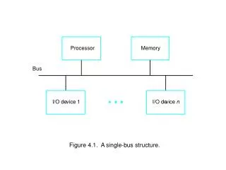
Components of any Computer System • Control – logic that controls fetching/execution of instructions • Memory – area where instructions/data are stored • Input/Output – external interaction with computer Address bus Control Memory Data bus Input/Outputdevices Blog: aforajayshahnirma.wordpress.com
Microprocessors First microprocessors placed control, registers, arithmetic logic unit in one integrated circuit (one chip). Data Bus CPU(ALU +Reg +control) Address Bus Memory I/O Devices Control Bus CPU – Central Processing Unit Blog: aforajayshahnirma.wordpress.com
Intel x86 Processors • In this chapter will study the Intel x86 general purpose microprocessor family • Instruction set architecture • Assembly language programming • Hardware features of different x86 implementations • Other features of microprocessor systems Blog: aforajayshahnirma.wordpress.com
The 8086 Microprocessor Family • Characteristics 1)16 bit microprocessor • It means all instructions and registers are operate with 16 bit. 2)16 bit data bus • it can read from or write to memory and I/O ports either 8 or 16 bits at a time 3)20 bit address bus • it can address 220 memory locations • each location is 1 byte (8 bits) wide, thus 16 bit words will require consecutive memory locations Blog: aforajayshahnirma.wordpress.com
4) 8086 includes few features, which enhance multiprocessing capability (it can be used with math coprocessors like 8087, I/O processor 8089 etc. 5) Operates on +5v supply and single phase (single line) clock frequency.(Clock is generated by separate peripheral chip 8284). 6) 8086 comes with different versions. 8086 runs at 5 MHz, 8086-2 runs at 8 MHz, 8086-1 runs at 10 MHz 7) It comes in 40-pin configuration with MOS technology having around 20,000 transistors in its circuitry. Blog: aforajayshahnirma.wordpress.com
Intel x86 Microprocessors 8086 - 20 bit Addr. Bus - 1MB of Memory 80286 - 24 Addr. Bus - Added Protection Mode 80386 - 32 bit regs/busses - Virtual 86 Mode 80486 - RISC Core - L1 Cache - FPU Pentium - Superscalar - Dual Pipeline - Split L1 Cache Pentium Pro - L2 Cache - Branch Pred. - Speculative Exec. Pentium MMX - 57 Instructions - Integrated DSP (MMX) Pentium II - 100 MHz Bus - L2 Cache - MMX Celeron - 66 MHz Bus - True L2 Cache Integration Pentium III - 100 MHz Bus - 70 Internet Streaming SIMD Ext. Blog: aforajayshahnirma.wordpress.com
Processor Architecture Components • Registers : used for storing data values and addresses • Execution units: perform computations (arithmetic, logic) on data • ALU: Arithmetic Logic Unit • Control: logic for fetching, executing instructions • Memory: stores instruction and data • Input/output: external interface with computer system • Instruction Queue: Pipelining
Architecture • The 8086 has two parts, the Bus Interface Unit (BIU) and the Execution Unit (EU). • The BIU fetches instructions, reads and writes data, and computes the 20-bit address. • The EUdecodes and executes the instructions using the 16-bit ALU. • Both units operate asynchronously to give the 8086 an overlapping instruction fetch and execution mechanism which is called as Pipelining. This results in efficient use of the system bus and system performance.
Bus Interface Unit • The bus interface unit is responsible for performing all external bus operations. Specifically it has the following functions: • Instruction fetch, Instruction queuing, Operand fetch and storage, Address relocation and Bus control. • The BIU uses a mechanism known as an instruction stream queue to implement a pipeline architecture. • This queue permits prefetch of up to six bytes of instruction code. When ever the queue of the BIU is not full, it has room for at least two more bytes and at the same time the EU is not requesting it to read or write operands from memory, the BIU is free to look ahead in the program by prefetching the next sequential instruction.
• These prefetching instructions are held in its FIFO queue. With its 16 bit data bus, the BIU fetches two instruction bytes in a single memory cycle. • After a byte is loaded at the input end of the queue, it automatically shifts up through the FIFO to the empty location nearest the output.
The BIU also contains a dedicated adder which is used to generate the 20 bit physical address that is output on the address bus. This address is formed by adding an appended 16 bit segment address and a 16 bit offset address. • For example, the physical address of the next instruction to be fetched is formed by combining the current contents of the code segment CS register and the current contents of the instruction pointer IP register. • The BIU is also responsible for generating bus control signals such as those for memory read or write and I/O read or write.
Generation of 20 bit physical address The 20-bit Physical address is often represented as, Segment Base : Offset OR CS : IP CS = 3480h IP=1234 CS 3 4 8 0 0 with Implied Zero + IP 1 2 3 4 ----------------------- 3 5 A3 4 H
AH AL General purpose register BH BL CH CL DH DL SP BP SI ALU Data bus (16 bits) DI ALU EU control instruction 1011000101001010 Flag register EU Operation Depending on the control signal, EU performs one of the following operations: • An arithmetic operation • A logic operation • Storing a data into a register • Moving a data from a register • Changing flag register
EXECUTION UNIT • The Execution unit is responsible for decoding and executing all instructions. • The EU extracts instructions from the top of the queue in the BIU, decodes them, generates operands if necessary, passes them to the BIU and requests it to perform the read or write bys cycles to memory or I/O and perform the operation specified by the instruction on the operands. • During the execution of the instruction, the EU tests the status and control flags and updates them based on the results of executing the instruction. • If the BIU is already in the process of fetching an instruction when the EU request it to read or write operands from memory or I/O, the BIUfirstcompletes the instruction fetch bus cycle before initiating the operand read / write cycle.
If the queue is empty, the EU waits for the next instruction byte to be fetched and shifted to top of the queue. • When the EU executes a branch or jump instruction, it transfers control to a location corresponding to another set of sequential instructions. • Whenever this happens, the BIU automatically resets the queue and then begins to fetch instructions from this new location to refill the queue.
A B n bits n bits Carry Y= 0 ? F A > B ? Y Arithmetic Logic Unit (ALU) F Y 0 0 0 A + B 0 0 1 A - B 0 1 0 A - 1 0 1 1 A and B 1 0 0 A or B 1 0 1 not A • Signal F control which function will be conducted by ALU. • Signal F is generated according to the current instruction. • Basic arithmetic operations: addition, subtraction, • Basic logic operations: and, or, xor, shifting,
Flag register 15 14 13 12 11 10 9 8 7 6 5 4 3 2 1 0 - - - - - - - O D I T S Z A P C Occurrence of Overflow Carry (Out from digit 7 or digit 15 Even Parity (error detection) Direction of Change of SI, DI Auxiliary carry (digit 3 carry into digit 4 generates) Maskable-Interrupt enable Trap (halt) Execution Zero result Sign (MSB) of result • Flag register contains information reflecting the current status of a microprocessor. A flag is a flip-flop which indicates some condition produced by executing an instruction, or controls certain operations
Status Flags Indicate Current Processor Status CF Carry Flag Arithmetic Carry/Borrow OF Overflow Flag Arithmetic Overflow ZF Zero Flag Zero Result; Equal Compare SF Sign Flag Negative Result; Non-Equal Compare PF Parity Flag Even Number of “1” bits AF Auxiliary Carry Used with BCD Arithmetic • Status and Control Bits Maintained in Flags Register • Generally Set and Tested Individually • 9 1-bit flags in 8086; 7 are unused
Control Flags Influence the 8086 During Execution Phase DF Direction Flag Auto-Increment/Decrement • used for “string operations” IF Interrupt Flag Enables Interrupts • allows “fetch-execute” to be interrupted TF Trap Flag Allows Single-Step • for debugging; causes interrupt after each operation
8086 Register File 7 0 7 0 AL BL CL DL AH BH CH DH Accumulator AX BX CX DX Base Counter Data 15 0 Code Segment CS DS SS ES Data Segment Stack Segment Extra Segment 15 0 } Instruction Pointer IP SP BP SI DI } Stack Pointer Base Pointer } Source Index Destination Index
General Purpose RegistersAX, BX, CX, DX 7 0 7 0 AX BX CX DX Accumulator AH BH CH DH AL BL CL DL Base • Can Be Used Separately as 1-byte Registers AX = AH:AL • Temporary Storage to Avoid Memory Access • Faster Execution • Avoids Memory Access • Some Special uses for Certain Instructions Counter Data
AX, BX, CX, DX - Some Specialized Uses 7 0 7 0 AX BX CX DX AL BL CL DL AH BH CH DH Accumulator Base Counter Data • AX, Accumulator • Main Register for Performing Arithmetic • mul/div must use AH, AL • “accumulator” Means Register with Simple ALU • BX, Base • Point to Translation Table in Memory • Holds Memory Offsets; Function Calls • CX, Counter • Index Counter for Loop Control • DX, Data • After Integer Division Execution - Holds Remainder
Data Read/Write process from /To Memory • Word Read • - Each of 1 MB memory address of 8086 represents a byte wide location • - 16 bit words will be stored in two consecutive Memory location • If first byte of the data is stored at an even address , 8086 can read the entire word in one operation. • o For example if the 16 bit data is stored at even address 00520H is 2607 • MOV BX, [00520] • 8086 reads the first byte and stores the data in BL and reads the 2nd byte and stores the data in BH • BL (00520) • BH (00521) 8086 reads the first byte from 00520 location and stores the data in BL and reads the 2nd byte from the 00521 location and stores it BH
If the first byte of the data is stored at an ODD address, 8086 needs two operation to read the 16 bit data o For example if the 16 bit data is stored at an odd address 00521H is F520 MOV BX, [00521] In first operation , 8086 reads the 16 bit data from the 00521 location and stores the data of 00521 location in register BL and discards the data of 00520 location In 2nd operation, 8086 reads the 16 bit data from the 00522 location and stores the data of 00522 location in register BH and discards the data of 00523 location BL (00521) BH (00522) For Odd Address MOV BH, [Addr] Ex: MOV BH, [ 00521] 8086 reads the first byte from 00520 location and ignores it and reads the 2nd byte from the 00521 location and stores the data in BH
Advantages of memory segmentation • Allow the memory capacity to be 1Mb even though the addresses associated with the individual instructions are only 16 bits wide. • Facilitate the use of separate memory areas for the program, its data, code and the stack. • Easier to manipulate 16 bit numbers than 20 bit numbers…one less byte to deal with. • Permit a program and/or its data to be put into different areas of memory each time the program is executed.
Memory FFFFF 59000 58FFF Extra 49000 48FFF 4 9 0 0 ES 44000 43FFF Stack 3 4 0 0 34000 33FFF SS 30000 2FFFF Code 2 0 0 0 CS 20000 1FFFF Data 1 0 0 0 DS 10000 0FFFF 00000
Segment Registers • Some of the 220 bytes of addresses are divided in to 4 64KB segments • code segment - CS register stores upper 16 bits of its starting address • where instructions are coming from • stack segment - SS register stores upper 16 bits of its starting address • stores addresses and data while a subprogram is executed • data segment - DS register stores upper 16 bits of its starting address • holds data • extra segment - ES register stores upper 16 bits of its starting address • holds more data • the lower 4 bits are always zero! why? • example: if, the starting address of the code segment is 348A0, then CS contains the value 348AH...this is called the segment base. • the segments can overlap in the case of small program
CS, DS, ES, SS - Segment Registers Contains “Index Value” for Memory Address Contains “Base Value” for Memory Address • CS, Code Segment------------------------------- • Used to “point” to Instructions • Determines a Memory Address • (along with IP) • Segmented Address written as CS:IP • DS, Data Segment-------------------------------- • Used to “point” to Data • Determines Memory Address • (along with other registers) • ES, Extra Segment ------------------------------------ • allows 2 Data Address Registers • SS, Stack Segment • Used to “point” to Data in Stack Structure (LIFO) • Used with SP or BP • SS:SP or SS:BP are valid Segmented Addresses • IP, Instruction Pointer • Used to “point” to Instructions • Determines a Memory Address (along with CS) • Segmented Address written as CS:IP • SI, Source Index; DI, Destination Index • Used to “point” to Data • Determines Memory Address (along with registers) • DS, ES commonly used • SP, Stack Pointer; BP, Base Pointer • Used to “point” to Data in Stack Structure (LIFO) • Used with SS • SS:SP or SS:BP are valid Segmented Addresses These can also be used as General Registers !!!!!!
Instruction Pointer Register 15 0 • IP Contains Address of NEXT Instruction to be Fetched • Automatically Incremented • Programmer can control with jump and branch
0000 Segment address + Offset Memory address 3 4 8 A 0 5 0 0 0 0 CS SS 4 2 1 4 F F E 0 IP + SP + Instruction address 3 8 A B 4 Stack address 5 F F E 0 1 2 3 4 0 DS 0 0 2 2 DI + Data address 1 2 3 6 2 Memory Address Calculation • Segment addresses must be stored in segment registers • Offset is derivedfrom the combination of pointer registers, the Instruction Pointer (IP), and immediate values • Examples
Generating Memory Addresses • How can a 16-bit microprocessor generate 20-bit memory addresses? Left shift 4 bits FFFFF 16-bit register 0000 Addr1 + 0FFFF Segment (64K) + 16-bit register Offset Offset Addr1 20-bit memory address Segment address 00000 1M memory space Intel 80x86 memory address generation
8086 Memory CS 1 2 3 4 IP 0 0 1 2 12352 MOV AL, 0 1 2 3 5 2 Fetching Instructions • Where to fetch the next instruction? • Update IP • After an instruction is fetched, Register IP is updated as follows: IP = IP + Length of the fetched instruction • For Example: the length of MOV AL, 0 is 2 bytes. After fetching this instruction, the IP is updated to 0014
1 2 3 4 0 (assume DS=1234H) DS 0 3 0 0 Memory address 1 2 6 4 0 (assume DS=1234H) 1 2 3 4 0 DS 0 3 1 0 (assume SI=0310H) Memory address 1 2 6 5 0 Accessing Data Memory • There is a number of methods to generate the memory address when accessing data memory. These methods are referred to as Addressing Modes • Examples: • Direct addressing: MOV AL, [0300H] • Register indirect addressing: MOV AL, [SI]
Interrupt pointer table Reserved Memory Locations • Some memory locations are reserved for special purposes. Programs should not be loaded in these areas FFFFF • Locations fromFFFF0H to FFFFFH are used for system reset code Reset instruction area FFFF0 • Locations from00000H to 003FFH are used for the interrupt pointer table • It has 256 table entries • Each table entry is 4 bytes 003FF 256 4 = 1024 = memory addressing space From 00000H to 003FFH 00000
A 64K segment Real-Mode memory address space 20 bit physical address value 1FFFF The offset or distance of this byte from the segment register is F000, its address is written as 1000:F000 1F000 Segment value In, say, CS, DS, SS, ES etc. Distance=F000 Segment register Offset register’s value, say the one in IP or SP. 1 0 0 0 10000 A segment register refers to a fixed memory location, whose address value= 10h * value of the segment reg. An offset pointer register (say, IP or SP) is used to hold the distance or offset value of a byte within the segment; when the IP or SP is varied, different locations within the Segment are referred to. To be replaced by next floid
Real mode memory FFFFF This location has an effect (distance in bytes) equal to F000 relative to the location pointed by the segment register shown below. 1FFFF Offset = F000 1F000 64-Kbyte segment Segment register Segment register is usually fixed at a value referring to a fixed location memory while the offset pointer register (e.g. IP, SP, etc.) is varied from time to time according to the program logic. 10000 1 0 0 0 00000
Ambiguous size operands Use PTR to resolve mov [bx],1 mov word ptr [bx],1 mov [si], 'A' mov [si],byte ptr 'A' X label byte M label word DW 100 X and M refer to the same address mov AH,X mov AH,byte ptr M mov AX,M PTR and LABEL
... A3 20 FF 17 5F ... 003A SP Access to the Stack • mov bp,sp ;BP points to stack top • mov ax,[bp+0] ;top of stack • mov bx,[bp+2] ;next to top of stack • mov [bp+3],ah ;byte at offset 3 in stack • mov [bp-1],ch ;byte above top of stack
Assuming that SP=1236, AX=24B6, D1=85C2, and DX=SF93, show the contents of the stack as each of the following instructions is executed: PUSH AX PUSH DI PUSH DX Solution: 93 SS:1230 5F SS:1231 C2 C2 SS:1232 85 85 SS:1233 B6 B6 B6 SS:1234 24 24 24 SS:1235 SS:1236 After PUSH AX SP=1234 After PUSH DI SP=1232 After PUSH DX SP=1230 START SP=1236 Example Assuming that the stack is as shown below, and SP=18FA, show the contents of the stack and Registers as each of the following instructions is executed: POP CX POP DXPOP BX Solution: 23 SS:18FA 14 SS:18FB 6B 6B SS:18FC 2C 2C SS:18FD 91 91 91 SS:18FE F6 F6 F6 SS:18FF SS:1900 After POP CX SP=18FC CX=1423 After POP DX SP=18FE DX2068 After POP BX SP=1900 BX=F691 START SP=18FA
Operand Types Operands are generally considered to be of 3 different types: immediate register memory Animmediate operand is a constant. A register operand is one of the CPU registers. A memory operand is a reference to a location in memory. The 8086 architecture provides 6 possible ways for specifying a memory operand: direct direct-offset register-indirect indexed base-indexed base-indexed with displacement
direct is the offset of a variable. count db 20 mov al, count mov bx, offset count direct-offset is the sum of a variable’s offset and a displacement arrayB db 12, 14, 16, 18 arrayW dw 1000H, 2000H, 3000H mov al, arrayB + 1 mov ah, arrayB + 2 mov ax, arrayW + 2 mov bx, arrayW + 4 register-indirect a register that contains the offset of data in memory. Only the SI, DI, BX, and BP registers can be used as indirect operands. astring db “abcdef” mov bx, offset astring add bx, 5 mov dl, [bx]
indexed is the sum of a base or index register and a displacement mov ax, arrayW[si] mov ax, arrayW[bx] base-indexed is the sum of a base register and an index register mov ax, [bx+si] mov ax, [bx][si] base-indexed with displacement is the sum of a base register, and index register, and a displacement mov ax, [bx+si+2] mov ax, arrayW[bx][si]
8086 Addressing Modes • There are 24 different addressing modes! • Fortunately, they break down into a smaller number of distinctive categories • Addressing Mode means how the address information in the instruction is used to select a physical address • Increase flexibility of programming language • Common modes specify one or more of Base register, Index register, and Displacement
Addressing modes • specify the different ways the processor can access data. • immediate addressing mode • Data accessed quickly from queue. No need of external bus. Data is a part of instruction. • MOV CX, 437BH • puts the specified value, 437BH directly into CX • register addressing mode • Fastest and compact. No need of external bus. • MOV CX, AX • a register is the source of the operand. • Implicit addressing mode • Data is in a predefined register like in a flag register. • STD , CLC are called zero address instruction.
Memory Addressing modes • Memory operands must be transferred from cpu over the bus. • Whenever EU need to read/write operand it must pass an offset value to BIU. • BIU generates 20 bit address. • EU calculates EA by summing displacement, content of base register, and index register.
Direct addressing mode Effective address is taken from displacement field of instruction. • MOV CX, [437AH] • MOV [437AH], CX Content of CX are copied to memory location whose offset is[437A]
Register Indirect • Offset is contained in a register - it is a pointer to a memory location • BP, BX, SI, DI only • The segment register is implied or may be specified. • mov ax,[bp] • movcl,es:[bx] • movdl,ds:[si] • mov [di],ax • By default DSis assumed for BX, SI, and DI • SS is assumed for BP • Advantage: one instruction can operate on many different location if value in base/index register is updated.