Processor
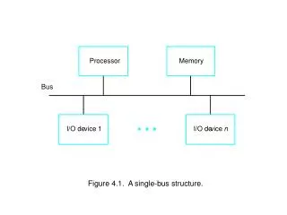
Processor. Memory. Bus. I/O de. vice 1. I/O de. vice. n. Figure 4.1. A single-bus structure. Mo. v. e. #LINE,R0. Initialize. memory. p. oin. ter. W. AITK. T. estBit. #0,ST. A. TUS. T. est. SIN. Branc. h=0. W. AITK. W. ait. for. c. haracter. to. b. e. en.

Processor
E N D
Presentation Transcript
Processor Memory Bus I/O de vice 1 I/O de vice n Figure 4.1. A single-bus structure.
Mo v e #LINE,R0 Initialize memory p oin ter. W AITK T estBit #0,ST A TUS T est SIN. Branc h=0 W AITK W ait for c haracter to b e en tered. Mo v e D A T AIN,R1 Read c haracter. W AITD T estBit #1,ST A TUS T est SOUT. Branc h=0 W AITD W ait for displa y to b ecome ready . Mo v e R1,D A T A OUT Send c haracter to displa y . Mo v e R1,(R0)+ Store c haracter and adv ance p oin ter. Compare #$0D,R1 Chec k if Carriage Return. Branc h 0 W AITK If not, get another c haracter. Mo v e #$0A,D A T A OUT Otherwise, send Line F eed. Call PR OCESS Call a subroutine to pro cess the input line. Figure 4.4 A program that reads one line from the keyboard stores it in memory buffer, and echoes it back to the display.
V dd Processor R I N T R INTR INTR1 INTR2 INTR n Figure 4.6. An equivalent circuit for an open-drain bus used to implement a common interrupt-request line.
Figure 4.7. Implementation of interrupt priority using individual interrupt-request and acknowledge lines.
Main Program Mo v e #LINE,PNTR Initialize buffer p oin ter. Clear EOL Clear end-of-line indicator. BitSet #2,CONTR OL Enable k eyb oard in terrupts. BitSet #9,PS Set in terrupt-enable bit in the PS. . . . In terrupt-service routine – READ Mo v eMultiple R0-R1, (SP) Sa v e registers R0 and R1 on stac k. Mo v e PNTR,R0 Load address p oin ter. Mo v eByte D A T AIN,R1 Get input c haracter and Mo v eByte R1,(R0)+ store it in memory . Mo v e R0,PNTR Up date p oin ter. CompareByte #$0D,R1 Chec k if Carriage Return. 0 Branc h R TRN Mo v e #1,EOL Indicate end of line. BitClear #2,CONTR OL Disable k eyb oard in terrupts. R TRN Mo v eMultiple (SP)+,R0-R1 Restore registers R0 and R1. Return-from-in terrupt Figure 4.9. Using interrupts to read a line of characters from a keyboard via the registers in Figure 4.3.
Figure 4.21. Sequence of signals during transfer of bus mastership for the devices in Figure 4.20.
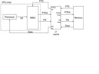
Bus D7 P A7 D A T AIN D1 D0 P A0 SIN Input CA status PB7 D A T A OUT PB0 SOUT CB1 Handshak e control CB2 Sla v e- 1 Ready Master - Ready R / W A31 My-address Address decoder A2 RS1 A1 RS0 A0 Figure 4.33. Combined input/output interface circuit.
D A T A OUT D7 D Q 7 7 Printer data D0 D Q 1 1 D0 D Q 0 0 SOUT Idle Handshak e control V alid Read Load status data R/ W Sla v e- ready Go A31 My-address T iming Address Logic decoder A1 A0 Clock My-address Respond Idle Go=1 Figure 4.35. A parallel point interface for the bus of Figure 4.25, with a state-diagram for the timing logic.
T ime 1 2 3 Clock Address R/ W Data Go Sla v e-ready Figure 4.36. T iming for the output interf ace in Figure 4.35.