Viterbi Decoder Project
Viterbi Decoder Project. Alon weinberg, Dan Elran Supervisors: Emilia Burlak, Sara Galan. General.

Viterbi Decoder Project
E N D
Presentation Transcript
Viterbi Decoder Project Alon weinberg, Dan Elran Supervisors: Emilia Burlak, Sara Galan
General In this project we implement the Viterbi Digital channel decoding algorithm in hardware on a Qualcomm Israel based platform, in order to learn about digital communication channels, the algorithm itself and the board
Project Goals • Studying the Viterbi algorithm and the convolutional code • Viterbi decoder implementation • Studying the board on which the implementation will take place • Studying the TI DSP on board • Studying the arbiter and busses (synch. And async.) on board • PCI bus and interface • H\W – Software interface (DSP – FPGAs) • Async. RAM model configuration • Async. RAM interface module implementation • Working in high frequencies (theory+implementation) • Good VHDL programming knowledge and abilities
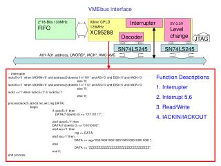
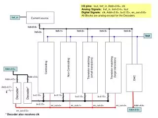
Board usage We implement the Viterbi decoder on one FPGA, using the two RAMs on board as input and output FIFOs for the decoder. There are also a couple of RAMs on the FPGA itself, in order to pass data between the various blocks (ACS\Chainback) and store temporary data.
Board bus rates • DSP works at 160 MHz • BUT Arbiter works at 40 MHz (Bottleneck) • Periferial BUS (PCI) • Local Bus • PLX and DSP can master both buses • Asynched I/O RAMs connected to FPGAs
Viterbi Decoding Algorithm • The Viterbi decoding algorithm is a state of the art algorithm used to decode convolutional binary codes (viewd as a trellis tree) used in communication standards (like Qualcomm’s CDMA standard). • The Viterbi decoder operates by finding the most likely decoding sequence for an input code symbol stream.
Convolutional codes Convolutional codes add correlation to the input data sequence by using delay elements and modulo adders. Binary convolutional encoders can be implemented with a feed forward shift register and exclusive or (XOR) gates.
Convolutional codes (cont.) Input bits enter the shift register one bit at a time. The outputs of the generator functions become the encoded output symbols. Each of the generator functions produce an output symbol for each input bit. The number of delay elements in the SHR define the state of the encoder and the constraint length. An encoder containing N memory elements has 2^N possible states and a K=N+1 constraint length.
Viterbi Decoding The Viterbi decoder finds the most likely path through the encoder Trellis. The 3 main steps in the process are : • Branch metric generation • State metric generation • Chainback
Implementation considerations • Fully parallel- N Trellis states are processed in parallel and each cycle a whole Trellis column is ready. This way we can also calculate the most likely state during the process and only output the decision bit. Easy for H/W implementation, fast. Takes a lot of FPGA space and resources (exponential with K). Not commonly used.
Implementation considerations (cont.) • Fully serial- each cycle one state is ready. N cycles to process one whole Trellis column. More difficult H/W implementation, N times slower. Takes a little FPGA space without any correlation to K (fixed amount of space taken). • Partially parallel- m<N states processed each cycle. Choose m by space and speed considerations (bigger m: faster, more space).
Implementation considerations (cont.) Since the chip is used in a mobile cellular phone, it should be very small, but still fast enough in order to prevent delays in the data stream (the conversation). Today most of the implementations are partially parallel, with a small m (2- 4). We chose the m=2 implementation (one butterfly), which has good speed-space payload. This implementation is scalable and can be very easily upgraded to a m=4/8 implementation by adding similar butterflies.
Software The software runs on the DSP, over the VX Works operating systems (which is the real time operating systems used on the CPU card).
Software (cont.) • The software has general control of the whole process (control the H/W through the control registers). • Originally, the chainback block should have been implemented in software on the DSP. Due to efficiency considerations this block is implemented in HW on the FPGA
Board and Bus Load • The async. bus between the FPGA and the DSP is a 40MHz bus (optimal). It was designed only to pass status and commands between the DSP and the FPGA. • In our implementation, ALL of the channel data on its way from the ACS block (on FPGA) to the Chainback block (on DSP) should have also been passed on this bus
Board and Bus Load (II) • Since the DSP works @ 160MHz and the bus is only 40MHz max (and async.), the bus would have been a major bottleneck in the implementation.
Board and Bus Load (III) • ACS processes one channel data bit (represented as a trellis column = 32 bits) every 16 WCX8 cycles=512 ns. • The Bus would’ve passed one bit every 25 ns => 800 ns to pass the whole trellis column (=1 channel data bit). • The DSP executes one command every 6.25ns. • Few commands needed for the Chainback block implementation.
Board and Bus Load (IV) • Therefore: Both the ACS (on the FPGA) and the Chainback (on DSP) would’ve had to wait for the bus. • Actually: It would probably be more efficient to implement the whole decoder in SW on the DSP than to implement it part HW and part SW using the 40MHz async. Bus. • Of course the fully HW implementation is the fastest and most efficient and speed scalable (although the most difficult one) • This is why the original “Chainback on DSP” design was abandoned, and the decoder was implemented fully on the FPGA. STILL the commands to the FPGA are passed through SW, and the whole SW-HW interface had to be studied
WHBI • All register writes in software reach the PLX, from there to the bus and then through the WHBI to the Viterbi registers (Run register and 8 WRAM Xface registers). The bus is a parallel bus- 16 bit data bus and 8 bit address bus.
WRAM Xface • This is the async. RAM interface. It has 4 registers: Mode, Address, Data, Limit. • The xface has 4 modes of operation: Play- the RAM data is played on the data bus, starting at the address entered at the address register until reaching the RAMs end address Play cylic- playing starts from the address at address reg. Until the address at limit reg in a cyclic way CPU access- each read/write to the data reg will cause a read/write to the address indicated at the address reg. The address in the address reg is incremented Record- the data on the data bus is recorded into the RAM, starting at the address indicated by the address register, until reaching the RAM end address
Branch Metric • Every channel data bit is represented by 2 bits after encoding. On the receiving side, these two bits enter a demodulator which outputs two numbers in the range of [-128,127]. These are the BMs’ inputs from the FIFO. The BM calculates the metrics for each branch. • To save FPGA space, the BM block is reduced to 4 MUX components of 4 inputs each, instead of one 16 input MUX which gives better LUTs usage. • Since it turns out that all 4 variations of possible branch probabilities are outputed, only in different order each time- we save calculations by always calculating the 4 possibilities and then choosing which possibility goes to which output by the 4 MUX components • Overall this block took 120 LUTs, 52 DFFs.
State Metric Control • Our decoder has a 32 states per column. • A general decoder usually has more states per column (~512) • The trivial solution to save the metrics would seem to be simple registers • BUT if our decoder is to be upgraded to more states per column- we’ll need a lot more registers, and a lot more FPGA space
State Metric Control (II) • Therefore we use 2 DPRs- one for the old metrics and one for the new ones (The DPRs switch roles each time- very complex address manipulations) . This implementation saves FPGA space, especially if the decoder is to be enlarged (and then all that has to be done is to enlarge the DPRs- saves space and VHDL code- 74 LUTs, 45 DFFs). • DPRs and not simple RAMS- enable simultaneous accesses to the metrics, which enable the ACS butterfly (a butterfly reads 2 metrics and writes 2 other metrics every clock cycle)
Add, Compare, Select • We used a one butterfly ACS- saves half the RAM accesses, speeds up the operation by 2. • Again- 5 MUX components of 4 inputs instead of 1 big 64->2 MUX- saves CLBs. (using 4->1 MUX components with 16 bit inputs, instead of 8->1 MUX of 8 bit inputs saves us some more space) • The ACS took: Area (LUTs) DFFs 254 178
ACS-Chainback interface • The theoretical assumption (used in order to save HW space) is that a chainback pass that starts and ends at the zero state is as accurate as the regular one, as long as the chainback pass is long enough. • For a one butterfly (2 bits output each cycle) a 52 columns deep chainback pass ensures almost perfect accuracy.
ACS-Chainback interface (II) • The ACS processes 2 bits of data every WCX8 cycle, i.e 16 cycles to process one 32 bit trellis column. • The Chainback reads one trellis column (represented as a 32 bit word) every cycle. • Therefore a 52 deep chainback pass takes 52 cycles, in which the ACS processes another 3.25 new columns. Since the CB has to wait another 12 cycles for the ACS to finish processing the 4th column, we decided to use a 64 columns deep chainback pass, which takes the same time but increases the accuracy
ACS-Chainback interface (III) • Therefore: The chainback processes 64 columns in 64 cycles. During this time the ACS processes 4 new columns. Overall we need a 68 columns deep RAM for the ACS-CB interface for best performance. • Since both a 64 columns deep RAM and a 128 deep one take the same number of block RAMs and space, but the 128 deep RAM prevents chainback stalls and ensures best performance-space payload, we are using a 128 cyclic DPRAM as the ACS-CB interface.
Chainback • 64 columns chainback depth- out of which the 4 last columns are probable enough to be written as output. • Therefore the pass on the CB DPR is 64->4, write 3->0, 68->8, write 7->4 etc. Also, the Ram is cyclic- overall complex address manipulation, while trying to minimize the FPGA space occupation.
Chainback (II) • For a 32 states column, 2 possible inputs for each state- over all 64 options, I.e a 64->1 MUX needed (can be reduced to smaller MUX components, as in ACS and BM) • Viewing the states as 5 bit vectors, and representing the branch taken (=decision bit) to each state as ‘0’ for upper branch, ‘1’ for lower branch, it turns out the the 4 LSBs of the present state concated to the decision bit as the new LSB, we get the previous state. That way we don’t need any MUX components at all !!! • Overall this block took 59 LUTs and 71 DFFs
FPGA Utilization • Design Summary: Number of Slices: 779 out of 12,288 6% Number of Slices containing unrelated logic: 0 out of 779 0% Number of Slice Flip Flops: 608 out of 24,576 2% Total Number 4 input LUTs: 1,010 out of 24,576 4% Number used as LUTs: 979 Number used as a route-thru: 12 Number used as Shift registers: 19 Number of bonded IOBs: 108 out of 404 26% IOB Flip Flops: 118 Number of Block RAMs: 4 out of 32 12% Number of GCLKs: 2 out of 4 50% Number of GCLKIOBs: 1 out of 4 25% Number of DLLs: 1 out of 4 25%Total equivalent gate count for design: 88,582Additional JTAG gate count for IOBs: 5,232