Download
1 / 48
480 likes | 731 Vues
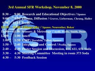
3rd Annual SFR Workshop, November 8, 2000. 8:30 – 9:00 Research and Educational Objectives / Spanos 9:00 – 9:50 Plasma, Diffusion / Graves, Lieberman, Cheung, Haller 9:50 – 10:10 break 10:10 – 11:00 Lithography / Spanos, Neureuther, Bokor

E N D
3rd Annual SFR Workshop, November 8, 2000 8:30 – 9:00 Research and Educational Objectives / Spanos 9:00 – 9:50 Plasma, Diffusion / Graves, Lieberman, Cheung, Haller 9:50 – 10:10 break 10:10 – 11:00 Lithography / Spanos, Neureuther, Bokor 11:00 – 11:50 Sensors & Metrology / Aydil, Poolla, Smith, Dunn 12:00 – 1:00 lunch 1:00 – 1:50 CMP / Dornfeld, Talbot, Spanos 1:50 – 2:40 Integration and Control / Poolla, Spanos 2:40 – 4:30 Poster Session and Discussion, 411, 611, 651 Soda 3:30 – 4:30 Steering Committee Meeting in room 373 Soda 4:30 – 5:30 Feedback Session
Lithography SFR Workshop November 8, 2000 Costas Spanos, Jeffrey Bokor, Andy Neureuther Berkeley, CA
Outline • Sensitivity of Scatterometry • Statistical Simulation and Optimization • Effects of line edge roughness • Novel lithography enhancements • Modeling and simulation
Sensitivity of Spectroscopic Scatterometry: Sub-100nm Technology SFR Workshop November 8, 2000 Ralph Foong, Costas Spanos Berkeley, CA
Why worry about the “limits” of Scatterometry? • Capabilities of scatterometry and required equipment specifications need to be formalized for 100nm metrology. • Commercial ellipsometers have been identified as being able to perform spectroscopic scatterometry. Hence, the focus of this study is on these equipment. • Precision of current generation commercial ellipsometers in measuring profiles consistent with 100nm technology node has to be confirmed. • Scalability of scatterometry towards 70nm and 50nm metrology has to be explored. • Minimum commercial ellipsometer specifications necessary to successfully implement 70nm and 50nm metrology need to be determined.
Overall Framework of Sensitivity Analysis EM Response Variations Tan Y Simulations for variation in parameter X [X(-),X(Nominal), X(+)] Lambda Profile Parameters Cos D Are Variations Detectable? Lambda NoYes Commercial Equipment Analysis Determine Noise Contributions Tan Y, Cos D Noise Spectrum Which part of the spectrum contains the most information?
Electromagnetic simulations are conducted for small changes in profile parameters to measure variations in EM response. Noise analysis of commercial ellipsometers is carried out to determine detectability of EM response variations. Methodology d(ISource) Rounding d(IDetector) Slope Angle d(qAnalyzer) PR CD Height Footing d(qPolarizer) ARC d(Beam Divergence) Poly-Si Sample Si
Signal averaged over 30 measurements Noise represents 1s standard deviation for each wavelength Empirical formula for signal-to-noise ratio: Noise = 0.412(Intensity)0.632 (R2 Value = 0.937) Signal-to-Noise Ratio for SOPRA Ellipsometer • Intensity fluctuation is the main contributor of measurement noise in ellipsometers. • Monte-Carlo simulations incorporating intensity fluctuations are used to determine the final distributions of Tan Y and Cos D. • The ‘Minimum Detectable Variation’ lines represent the sum of the 3s errors of each of the 2 profiles measured to obtain the variation. • The graphs demonstrate a trend toward significant information contained in a narrow band in the lower wavelength spectrum.
Detectable (Above yellow line) Undetectable (Below yellow line) 100nm Technology Simulations 100nm Dense Lines (ASIC) 65nm Isolated Lines (MPU) Detectable (Above yellow line) Undetectable (Below yellow line) spectrum of information content
Detectable (Above yellow line) Undetectable (Below yellow line) 70nm Technology Simulations 70nm Dense Lines (ASIC) 45nm Isolated Lines (MPU)
50nm Technology Simulations 50nm Dense Lines (ASIC) 30nm Isolated Lines (MPU) Detectable (Above yellow line) Undetectable (Below yellow line)
DUV Photolithography In-Line Scatterometry PR Deposition, Focus, Exposure, Bake Time, Development Time, etc Profile Diagnostics Wafers Process Flow Process Flow Scatterometry Milestones • Characterize the capabilities of scatterometry in fulfilling the metrology needs of the 100nm technology node, by 9/31/2001 • Study the feasibility of 100nm profile extraction using small footprint, in-line spectroscopic ellipsometry, by 9/31/2002 • Implement lithography controller that merges full profile in-line information with available metrology, by 9/31/2003 Feedback Control Loop
Process Monitoring and Optimization Using Simulation and Full-profile Metrology SFR Workshop November 8, 2000 Junwei Bao, Costas Spanos Berkeley, CA
Process Monitoring and Optimization Using Simulation and Full-profile Metrology • Lithography simulators are mainly used to study the qualitative effects and trends of certain parameters. • Importance of quantitative predictive capabilities is increasing with increasing development costs and time-to-market pressures. • Extremely small process window leads to unstable process. • More frequent and in-line measurement is needed to monitor process drift. • Process recipe needs to be optimized to maximize the yield considering the effect of parameter variations.
Experimental Simulator Tuning and Process Characterization • Design of Experiment • 24 wafers, patterned using focus-exposure matrix • Different softbake temperature, PEB temperature and time, develop time • Resist index variation due to bake temperature is very small – can be ignored for scatterometry library generation
Simulator Calibration using Full-profile Metrology • Full-profile information is needed for simulator calibration due to high-dimensionality and non-linearity of the parameter space. • Scatterometry • Non-destructive • High throughput and in-line capability • Full-profile information • Other full-profile metrologies • Applied Materials, VeraSEM™3D Metrology SEM™ • AFM • Cross-section SEM
Scatterometry Repeatability Characterization Using STI Structure Reproducibility: 10 consecutive measurements at same location with one time wafer loading Repeatability: Each measurements was performed on fresh loading on the same wafer Long-term data collected from June 9 to June 27
Process Monitoring using in-line Metrology Process Monitor based on tuned simulator resist thickness n & k thickness DITL resist profile reflectometer ellipsometer reflectometer scatterometer Exposure Develop Spin coat & softbake PEB
Yield Prediction • Distribution of equipment settings • Historical data obtained from equipment characterization • Estimated from simulator-process mismatch estimation • Process window calculation • Generate input parameter – output profile relation using calibrated simulator • Calculate process window according to profile constraint • Predicting Yield of lithography process by overlap integration
Process Window Engineering • Change the shape of the process window by adjusting the operating point settings and material parameters (if possible), so that the overlap integration between the joint p.d.f of inputs and the process window, i.e., the projected lithography yield, is maximized.
Parameter distributions In-die spatial variation Simulated Output distributions Profiles within spec. Calibrated Lithography Simulator Operating Point distributions + - Overlapping to get yield RECIPE OPTIMIZER Litho Control Milestones Demonstrate simulator tuning for full profile matching over a range of focus and exposure conditions by 9/30/2001. Demonstrate lithography simulator tuning for full statistical profile matching over a range of conditions by 9/30/2002. Implement lithography controller that merges full profile in-line information with available metrology by 9/30/2003.
Effects of LER on MOSFET Electrical Behavior SFR Workshop November 8, 2000 Shiying Xiong, Jeffrey Bokor Berkeley, CA
Motivation • Problems with LER • Channel length variation • Edge Electric field • Enhanced dopant diffusion • Possible effects on devices • Change of device parameters from target values • ( leakage, driving current, swing and etc.) • Enhanced hot carrier degradation • Isolation problem
LER device simulation • Base device design 0.1um SOI NMOSFET with self-aligned source and drain • Gate Length = 0.1um • Buried Oxide = 100 nm • Si Film Thickness = 250Å • Gate Oxide = 30 Å • Channel doping and halo selected to make Vt ~ 0.4V • Swing 70-80 mV/decade • Vdmax = 1.1V • LER model • Digitized red noise • LER parameters: • RMS • Correlation Length ( ~1/fcutoff )
Simulation results • Device with diffusion (Source side is rough) • After diffusion: • Junction is smoothed • Leff is reduced
Simulation Results • LER enhanced dopant diffusion • Junction extracted from device simulation • Further proof: 2D diffusion of doping boundary with LER Significant enhanced diffusion when Lc smaller or comparable with diffusion SQRT(Dt)
Do we really need 3D simulations? • 2D simulation of abrupt junction devices of different channel length Small
Starting experiments • Cooperation Project with AMD SEM current scan over line • step one: LER extraction Rebuilt of the top line edge of ~50nm bottom width line Average top width: 39.3nm, RMS1=2.5nm, RMS2=2.7nm, RMSW=2.7nm
Summary • Fast 2D simulation approach for LER effect was demonstrated • LER effect can be captured by 2D simulations • Range of validity for roughness correlation length under study • Collaboration on experiment with AMD finally underway • LER measurement protocols being developed Proposal Milestones • Complete simulations for AMD structures (bulk device with channel length 70nm or less) - FALL 2000 • AMD wafers complete to gate level (TBD) • Characterization of gate roughness (TBD) • AMD wafers out (TBD) • Device characterization (TBD)
Novel Lithography Enhancements and Modeling/Simulation SFR Review November 8th, 2000 Kostas Adam, Mosong Cheng, Andy Neureuther, Berkeley, CA
Threads, Objectives and Proposed Research • Novel Optical Lithography Enhancements Screen, quantify and reduce to practice techniques for enhancing feature resolution and reproducibility • Electric-field enhanced post-exposure bake • Defect-probe based aberration monitors • Polarization nanoimprinted masks • Simulation of Lithography Performance Quantify and provide models for the impact on lithographic performance of non-idealities in masks, optics and resists • 3D phase defects on phase-shifting masks • Roles of chemically-amplified resist and topography • Calibration of electromagnetic simulation tools ASML 248nm Experimental Test Bed
illumination plane quartz glass post underetch glass void defect height 180o phase shift d size feature (Cr) CDmask observation plane (near field) vacuum (air) 3D Phase Defect Printability: Approach Simulation with TEMPEST Illumination: Linearly polarized plane wave (TE/TM), l=248nm Imaging: Demagnification=4X, s=0.3, NA=0.68 The CDaerial is evaluated at the 30% level of the normalized intensity
3D Phase Defect Printability: Results – Near Field 160 x 160nm (4X) post |E| Phase of E 160 x 160nm (4X) void |E| Phase of E Glass posts and voids do not have the expected intensity and phase and this loosens and tightens defect tolerances.
Illumination: E Quartz geometrical position of edge Stack Air New edge location for ideal simulation 50nm New Model for Mask Edges: Approach Goal: Model the bias between ideal and rigorous simulations to allow use of the thin-mask approximation in design of OPC etc. New Model: Modify mask geometry that is input in an ideal SPLAT simulation. This can be done by extracting information from the near-field diffraction pattern of 2D rigorous simulations (TEMPEST). So far: New Model: In SPLAT Mask In SPLAT Mask a+Da a a a b +Db b b b
Inspection of Phase Defects The defect proximity to the feature affects both its inspectability and its printability Isolated quartz defect: Spatial variations of EM field (modes) 0o 180o Approach (similar to Socha’s contact hole inspection): - Excite a spatial mode within the defect and find the EM field outside - Time reversal: Use the calculated EM field as new illumination resulting EM field excite defect mode
Electric-Field-Enhanced Post Exposure Bake • A vertical electric field enhances the vertical drift/oscillation of the photoacid and thereby improves the profile verticality and reduces the lateral acid diffusion. • Al plates were coated with a film to prevent electrochemical reaction • E-field: AC component and an upward DC bias to reduce T-topping. UVIIHS. 0.3, 0.2, 0.1mm L/S, 12mC/cm2. PEB 140oC, 90s. Dev. 60s. EFE-PEB: AC 9.8V, DC 0.65V, 3Hz. Arrays Present Arrays Undercut and Gone Iso Lines Not Open Iso Line Open EFE-PEB Standard
Rapid Imaging Algorithm for Resist RIAR • 2-D reaction/diffusion time-evolving scheme • Approximate species by parabolic polynomials during a time-step. • Iteratively solve for the polynomial coefficients and reduce the time step until the error reaches certain criteria. CPU time of STORM=O(N2) CPU time of RIAR=O(N1.38) For 625 nodes, STORM 3min, RIAR 20sec. SPIE 00 Cheng
Line-End Shortening Modeling: Approach Line-end Shortening in 193nm Lithography: modeling and Simulation Mosong Cheng, Keeho Kim*, Mark Terry*, Maureen Hanratty*, Andrew Neureuther *KFAB PEMT PATTERN GROUP Texas Instruments TOOL DATA (Aberrations) MASK DATA OPTICAL SIM RESIST PARAM Sematech RESIST SIM 2D MASK DATA EXP. DATA (193 nm Tool SEM) Measured on Mask CD and LES - TUNE RESIST MODEL Analyze Discrepancy DESIGN SPECS MASK, RESIST, LENS.
Line-End Shortening Modeling: Results Simulation Compared to Exp. #2 l=193nm,NA=0.6, s=0.75, resist thickness=350nm, BARC thickness=82nm. Real mask CD data were used.
Comparison of the calibrated resist model to LES at defocus 0.2mm SEM picture PROLITH simulation
Defect-Probe Based Aberration Targets: Approach Dark Field Patterns Grid is 0.1 l/NA Probe Astigmatism Spherical 1 at 90o Trefoil Coma 1 at 0o 1 at 180o
Defect-Probe Based Aberration Targets: Results Trefoil Sensitivity 0.366 0.190 0.068 - Trefoil No Aberration + Trefoil
Polarization Nanoimprint Mask: Approach Polarization is a Remaining Frontier in Resolution Enhancement? Polarization orthogonal spillover Polarization adjusted half-tone Phase-shifted spillover Reduced Proximity Phase shift Half-Tone • Grating layers: step and flash lithography (UTA). • Freedom in image vs mask maker and equipment vendor bondage?
ASML Projection Printer: Tools and Status • ASML Model 90: l = 248 nm, NA = 0.52, s = flex • Donated by ASML to Berkeley • Cymer will assist with laser • Asyst providing mask pods and opener • VLSI donated SVG 8800 track • Shipley, Shen-Etsu donated materials • Status – Target Nov/Dec • Got it in Microlab! 7,000 lb, taller than ceilings • Track out for retrofitting • Room and gas handling underway • Masks: make 0.4 mm, buy some 0.3 mm, make some PSM
ASML Projection Printer: Research and Synergism • Image Quality • Aberrations including chromatic • Pattern dependent resolution enhancement • Polarization as a remaining degree of freedom • Resist Modeling and Line End Shortening • Resist parameters including diffusion • Role of resist and image quality on performance • Ultimate Resist Limits • Line edge roughness • Novel processing (Electric-field enhanced) • Novel materials (dendrimers)
Results and Plans: Novel Technologies • Novel Optical Lithography Enhancements • Electric-Field Enhanced Diff. – 3BEAMS M. Cheng • Field Strength, Polarity, Frequency, Resist Type • Defect-Probe Aberr. Targets– BACUS A. Neureuther • Tune sensitivity and orthogonality, Dry-lab, ASML verification • Polarization nanoimprinted masks • Simulate near fields and images, Dry-lab, ASML verification • Timetable and Milestones • Y1 Initial experiments and simulations to test concepts • Y2 Conduct and quantitatively interpret prototypes • Y3 Design apparatus, test procedures and data analysis ASML Stepper Installation and Experiments
Results and Plans: Modeling and Simulation • Simulation of Lithography Performance • OPC EM Analysis – SPIE K. Adam • 3D Phase-Defect EM Analysis – 3BEAMS K. Adam • Establish models; Assess impact of typical defects, • Invent alternative inspection approaches • Line End Shortening • Rapid Algorithms for Resist – SPIE M. Cheng • Combine tool aberration and resist models • Substrate topography effects • Timetable and Milestones • Y1 Determine importance of physical effects • Y2 Guidelines for 3D phase defects; Substrate in LES • Y2 Model defect inspection; Tool, resist, substrate LES ASML Stepper Installation and Experiments