Download
1 / 98
980 likes | 1.15k Vues
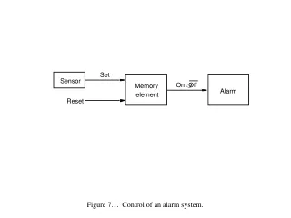
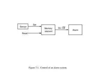
Set. Sensor. ¤. On. Off. Memory. Alarm. element. Reset. Figure 7.1. Control of an alarm system. A. B. Figure 7.2. A simple memory element. Load. A. B. Output. Data. TG1. TG2. Figure 7.3. A controlled memory element. Reset. Set. Q.

E N D
Set Sensor ¤ On Off Memory Alarm element Reset Figure 7.1. Control of an alarm system.
A B Figure 7.2. A simple memory element.
Load A B Output Data TG1 TG2 Figure 7.3. A controlled memory element.
Reset Set Q Figure 7.4. A memory element with NOR gates.
Q S R Q R a b Q a (no change) 0 0 0/11/0 0 1 0 1 1 0 1 0 1 1 0 0 Q b S (a) Circuit (b) Truth table t t t t t t t t t t 1 2 3 4 5 6 7 8 9 10 1 R 0 1 S 0 1 Q ? a 0 1 Q ? b 0 Time (c) Timing diagram Figure 7.5. A latch built with NOR gates.
Please see “portrait orientation” PowerPoint file for Chapter 7 Figure 7.6. Gated SR latch.
S Q Clk Q R Figure 7.7. Gated SR latch with NAND gates.
Please see “portrait orientation” PowerPoint file for Chapter 7 Figure 7.8. Gated D latch.
t su t h Clk D Q Figure 7.9. Setup and hold times.
Please see “portrait orientation” PowerPoint file for Chapter 7 Figure 7.10. Master-slave D flip-flop.
Q D Clock Q (b) Graphical symbol 1 P3 P1 2 5 Q Clock 6 Q P2 3 4 P4 D (a) Circuit Figure 7.11. A positive-edge-triggered D flip-flop.
Please see “portrait orientation” PowerPoint file for Chapter 7 Figure 7.12. Comparison of level-sensitive and edge-triggered.
Preset D Q Clock Q Clear (a) Circuit Preset Q D Q Clear (b) Graphical symbol Figure 7.13. Master-slave D flip-flop with Clear and Preset.
Please see “portrait orientation” PowerPoint file for Chapter 7 Figure 7.14. Positive-edge-triggered D flip-flop with Clear and Preset.
Please see “portrait orientation” PowerPoint file for Chapter 7 Figure 7.16. T flip-flop.
J Q D Q K Q Q Clock (a) Circuit Q ( t + 1 ) J K 0 0 Q ( t ) J Q 0 1 0 1 0 1 K Q 1 1 Q ( t ) (b) Truth table (c) Graphical symbol Figure 7.17. JK flip-flop.
Q Q Q Q 1 2 3 4 In Out Q Q Q Q D D D D Clock Q Q Q Q (a) Circuit Q Q Q Q = Out In 1 2 3 4 t 1 0 0 0 0 0 t 0 1 0 0 0 1 t 1 0 1 0 0 2 t 1 1 0 1 0 3 t 1 1 1 0 1 4 t 0 1 1 1 0 5 t 0 0 1 1 1 6 t 0 0 0 1 1 7 (b) A sample sequence Figure 7.18. A simple shift register.
Parallel output Q Q Q Q 3 2 1 0 Q Q Q Q D D D D Q Q Q Q Serial Clock Shift/Load input Parallel input Figure 7.19. Parallel access shift register.
1 Q Q Q T T T Clock Q Q Q Q Q Q 0 1 2 (a) Circuit Clock Q 0 Q 1 Q 2 Count 0 1 2 3 4 5 6 7 0 (b) Timing diagram Figure 7.20. A three-bit up-counter.
1 Q Q Q T T T Clock Q Q Q Q Q Q 0 1 2 (a) Circuit Clock Q 0 Q 1 Q 2 Count 0 7 6 5 4 3 2 1 0 (b) Timing diagram Figure 7.21. A three-bit down-counter.
Clock cycle Q Q Q 2 1 0 Q changes 1 0 0 0 0 Q changes 2 1 0 0 1 2 0 1 0 3 0 1 1 4 0 0 1 5 1 0 1 6 1 0 1 7 1 1 1 8 0 0 0 Table 7.1. Derivation of the synchronous up-counter.
1 Q Q Q Q T T T T Q Q Q Q 0 1 2 3 Clock Q Q Q Q (a) Circuit Clock Q 0 Q 1 Q 2 Q 3 Count 0 1 2 3 4 5 6 7 8 9 10 11 12 13 14 15 0 1 (b) Timing diagram Figure 7.22. A four-bit synchronous up-counter.
Enable Q Q Q Q T T T T Clock Q Q Q Q Clear Figure 7.23. Inclusion of Enable and Clear capability.
Please see “portrait orientation” PowerPoint file for Chapter 7 Figure 7.24. A four-bit counter with D flip-flops.
Please see “portrait orientation” PowerPoint file for Chapter 7 Figure 7.25. A counter with parallel-load capability.
Enable 1 D Q 0 0 0 D Q 0 1 1 D Q 0 2 2 Load Clock Clock (a) Circuit Clock Q 0 Q 1 Q 2 Count 0 1 2 3 4 5 0 1 (b) Timing diagram Figure 7.26. A modulo-6 counter with synchronous reset.
1 Q Q Q T T T Q Q Q 0 1 2 Clock Q Q Q (a) Circuit Clock Q 0 Q 1 Q 2 Count 0 1 2 3 4 5 0 1 2 (b) Timing diagram Figure 7.27. A modulo-6 counter with asynchronous reset.
Enable 1 D Q 0 0 0 D Q 0 1 1 BCD D Q 0 0 2 2 Q D 0 3 3 Load Clock Clock Enable Clear D Q 0 0 0 D Q 0 1 1 BCD 1 D Q 0 2 2 D Q 0 3 3 Load Clock Figure 7.28. A two-digit BCD counter.
Please see “portrait orientation” PowerPoint file for Chapter 7 Figure 7.29. Ring counter.
Q Q Q 0 1 n – 1 Q Q Q D D D Q Q Q Reset Clock Figure 7.30. Johnson counter.
Figure 7.31. Three types of storage elements in a schematic.
Data Clock Latch Figure 7.32. Gated D latch generated by CAD tools.
Please see “portrait orientation” PowerPoint file for Chapter 7 Figure 7.33. Implementation of a circuit in a CPLD.
module D_latch (D, Clk, Q); input D, Clk; output Q; reg Q; always @(D or Clk) if (Clk) Q = D; endmodule Figure 7.35. Code for a gated D latch.
module flipflop (D, Clock, Q); input D, Clock; output Q; reg Q; always @(posedge Clock) Q = D; endmodule Figure 7.36. Code for a D flip-flop.
module example7_3 (D, Clock, Q1, Q2); input D, Clock; output Q1, Q2; reg Q1, Q2; always @(posedge Clock) begin Q1 = D; Q2 = Q1; end Endmodule Figure 7.37. Incorrect code for two cascaded flip-flops.
module example7_4 (D, Clock, Q1, Q2); input D, Clock; output Q1, Q2; reg Q1, Q2; always @(posedge Clock) begin Q1 <= D; Q2 <= Q1; end endmodule Figure 7.39. Code for two cascaded flip-flops.
module example7_5 (x1, x2, x3, Clock, f, g); input x1, x2, x3, Clock; output f, g; reg f, g; always @(posedge Clock) begin f = x1 & x2; g = f | x3; end endmodule Figure 7.41. Code for Example 7.5.
module example7_6 (x1, x2, x3, Clock, f, g); input x1, x2, x3, Clock; output f, g; reg f, g; always @(posedge Clock) begin f <= x1 & x2; g <= f | x3; end endmodule Figure 7.43. Code for Example 7.6.
module flipflop (D, Clock, Resetn, Q); input D, Clock, Resetn; output Q; reg Q; always @(negedge Resetn or posedge Clock) if (!Resetn) Q <= 0; else Q <= D; endmodule Figure 7.45. D flip-flop with asynchronous reset.
module flipflop (D, Clock, Resetn, Q); input D, Clock, Resetn; output Q; reg Q; always @(posedge Clock) if (!Resetn) Q <= 0; else Q <= D; endmodule Figure 7.46. D flip-flop with synchronous reset.