Download
1 / 11
110 likes | 139 Vues
This text provides an introduction to semiconductor diodes, including their basic structure, operation under no bias, forward bias, and reverse bias conditions, as well as their characteristics. It also discusses the thermal voltage and ideality factor associated with diodes.

E N D
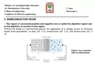
Ministry of teaching& high education Al- Mustansiriya University College of engineering Computer & Software engineering 1' class Electronic 1 5. SEMICONDUCTOR DIODE • This region of uncovered positive and negative ions is called the depletion region due to the depletion of carriers in this region. • Since the diode is a two-terminal device, the application of a voltage across its terminals leaves three possibilities: no bias (VD 0 V), forward bias (VD 0 V), and reverse bias (VD 0 V). Figure 1.9 p-n junction with no external bias.
No Applied Bias (VD = 0 V) • For the purposes of future discussions we shall assume that all the minority carriers of the n-type material that find themselves in the depletion region due to their random motion will pass directly into the p-type material. Similar discussion can be applied to the minority carriers (electrons) of the p-type material. This carrier flow has been indicated in Fig. 1.9 for the minority carriers of each material. However, the number of majority carriers is so large in the n-type material that there will invariably be a small number of majority carriers with sufficient kinetic energy to pass through the depletion region into the p-type material. Again, the same type of discussion can be applied to the majority carriers (holes) of the p-type material. The resulting flow due to the majority carriers is also shown in Fig. 1.9. • In the absence of an applied bias voltage, the net flow of charge in any one direction for a semiconductor diode is zero. • The symbol for a diode is repeated in Fig. 1.10 with the associated n- and p-type regions. Note that the arrow is associated with the p-type component and the bar with the n-type region. As indicated, for VD = 0 V, the current in any direction is 0 mA. Figure 1.10 No-bias conditions for a semiconductor diode.
Reverse-Bias Condition (VD ˂ 0 V) • If an external potential of V volts is applied across the p-n junction such that the positiveterminal is connected to the n-type material and the negative terminal is connectedto the p-type material as shown in Fig. 1.11, the number of uncovered positiveions in the depletion region of the n-type material will increase due to the largenumber of “free” electrons drawn to the positive potential of the applied voltage. • This widening of the depletion region will establish too great a barrier for the majority carriers toovercome, effectively reducing the majority carrier flow to zero as shown in Fig. 1.11. Figure 1.11 Reverse-biased p-n junction. • The current that exists under reverse-bias conditions is called the reverse saturation current and is represented by Is.
The term saturation comes from the fact that it reaches its maximum level quickly and does notchange significantly with increase in the reverse-bias potential, as shown on the diode characteristics of Fig. 1.14 for VD ˂ 0 V. • The reverse-biased conditions are depicted in Fig. 1.12 for the diode symbol and p-n junction. Note, in particular, that the direction of Is is against the arrow of the symbol. Fig.1.12 Reverse-bias conditions for a semiconductor diode. • Forward- Bias Condition (VD ˃ 0 V) • A forward-bias or “on” condition is established by applying the positive potential to the p-type material and the negative potential to the n-type material as shown in Fig. 1.13. For future reference, therefore: • A semiconductor diode is forward-biased when the association p-type and positive and n-type and negative has been established.
Figure 1.13 Forward-biased p-n junction. • The application of a forward-bias potential VD will “pressure” electrons in the n-type material and holes in the p-type material to recombine with the ions near the boundary and reduce the width of the depletion region as shown in Fig. 1.13.
sulting in an exponential rise in current as shown in the forward-bias region of the • characteristics of Fig. 1.14. Note that the vertical scale of Fig. 1.14 is measured in • milliamperes (although some semiconductor diodes will have a vertical scale measured • in amperes) and the horizontal scale in the forward-bias region has a maximum of 1 V. Typically, therefore, the voltage across a forward-biased diode will be less than 1 V. Note also, how quickly the current rises beyond the knee of the curve. • semiconductor diode can be defined by the following equation for the forward- and reverse-bias regions: • where: • Is = reverse saturation current. • VD: is the applied forward - bias voltage across the diode. • ɳ : is an ideality factor, which is a function of the operating conditions and physical construction; it has a range between 1 & 2 depending awide variety of factors • (ɳ =1 will be assumed throughout this text unless otherwise noted) • The voltage VT in Eq.(1-1) is called the thermal voltage is determined by: • Where: • K: is Boltzmann's constant = 1.38*10-23 J/K • T: is the absolute temperature in Kelvins = 273+temperture C0 • q: is the magnitude of electronic charge = 1.6*10-19 C
Example 1.1: At temperature of 270C (common temperature for components in an enclosed operating system). Determine the thermal voltage VT? Solution: Substituting in to Eq.(1 - 2), we obtain T = 273 + C0 = 273 + 27 = 300K For positive values of VD the first term of the above equation will grow very quickly atV = 0v, Eq.(1-1) becomes • For negative values of
Zener Region Fig 1.15 Zener region. • As the voltage across the diode increases in the reverse-bias region, the velocity of the minority carriers responsible for the reverse saturation current Is will also increase. Eventually, their velocity and associated kinetic energy (WK 12 mv2) will be sufficient to release additional carriers through collisions with otherwise stable atomic structures. • The avalanche region (VZ) can be brought closer to the vertical axis by increasing the doping levels in the p- and n-type materials. • However, as VZ decreases to very low levels, such as 5 V, another mechanism, called Zener breakdown. • The maximum reverse-bias potential that can be applied before entering the Zener region is called the peak inverse voltage (referred to simply as the PIV rating) or the peak reverse voltage (denoted by PRV rating).
Ge , Si & Ga As: • Forward characteristics : (Refer to the graph shown above). It is quite clear from the graph that the general shape of the curve for all three type of semiconductor diodes is same. However the threshold voltage of all the three diodes is different. The threshold voltage for Ge, Si, and GaAs diodes is 0.3, 0.7 and 1.2 V respectively. Thus if a Si diode is connected in a circuit in forward bias configuration, the voltage drop across the diode would be 0.7 V (assuming correct operation of diode). If Ge diode is used, then the voltage drop would be about 0.3 V and for GaAs diodes the voltage drop would be about 1.2 V. • Reverse characteristics : (Refer to the graph shown above). The characteristics curve of Ge, Si and GaAs diodes looks quite similar. However they are not same. The reverse saturation current of GaAs is least as compared to Si and Ge. The reverse saturation current of Si is more than that of Ge. Typical values of reverse saturation current are 1 pA, 10 pA and 1µA for GaAs, Si and Ge diodes respectively. • It is also clear from the above graph that the reverse breakdown voltage of all the three types of diodes are also different. The reverse breakdown voltage of GaAs is highest while that of Ge is lowest. Typical value of reverse breakdown voltage for Ge is less than 100 V, with maximum around 400 V. The reverse breakdown voltage of Si and GaAs diodes lies between 50 V and 1 kV.