Download
1 / 19
190 likes | 322 Vues
As signal integrity and speed demands rise in complex system architectures, backplane design faces unique challenges. This paper discusses the criticality of simulation tools in ensuring effective backplane designs, addressing issues such as loading conditions, parts selection, signal integrity, and crosstalk. By utilizing advanced simulation environments, designers can efficiently explore various design parameters and validate performance across diverse conditions. This includes examples demonstrating the impact of termination schemes on signal behavior, showcasing essential methodologies for achieving optimal backplane solutions.

E N D
Using Simulation Techniques to Guarantee Successful Backplane Design Shahana Aziz Muniz Engineering, INC MAPLD September 7-9, 2005
Introduction: • Backplane speeds are getting faster due to complex system architectures with high bandwidth • Complex systems now require larger number of loads, higher throughput and dense signal connectivity to meet project requirements. • Backplanes now operate at frequencies of hundreds of MHz, accommodating driver/receiver devices with fast edge rates • Successful backplane design requires careful analysis and simulation MAPLD2005/115
The Challenges of Backplane Design • Backplane design has additional challenges compared to a standalone circuit board deign • Need a design solution that can work across a range of multiple design variables • Plug-in cards may use different possible driver and receiver combinations • System may have a varying number of loads • Finding the optimal solution under a changing load condition is not a trivial problem • Simulation tools provide results for all corner cases quickly and accurately MAPLD2005/115
Simulation Tools Provide a Complete Solution • Tools provide a real world environment • Provide the capability to analyze how loading and parts selection effects issues such as undershoot, overshoot, ringing, crosstalk and timing • Makes it possible to decide about including or excluding termination solutions on the backplane, the choice of backplane trace impedance, backplane dimensions and slot distances and other design parameters • Provides feedback to the plug-in card designers such as driver/receiver component selection, termination schemes for those boards • Provides the environment of determining a complete system solution. • Capability to vary stimulus and models to simulate all possible corner cases, in order to validate circuit performance across all voltage and temperature ranges • Simulations in this paper were completing using Mentor Graphics’ Interconnectix Synthesis (IS) Analyzer and Multiboard, and Sigrity INC’s Speed2000. MAPLD2005/115
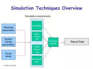
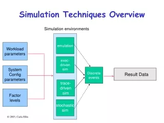
Simulation Environment Setup • The Backplane simulation environment is comprised of the following components: • Individual plug-in card simulation models • Backplane simulation model • Interconnection matrix • Device models • Noise rules and simulation stimulus MAPLD2005/115
Simulation Environment Setup Continued • Define System Connectivity • Plug-in cards can be included or excluded from the simulation to create different loading conditions • Specify connector pin matrix. Connection is made by pin number or net name • Import connector model to incorporate pin to pin contact parasitics MAPLD2005/115
Simulation Examples • Simulation was run to investigate the solution for problems such as: • Signal Integrity • Parts Selection • Timing • Crosstalk • Characteristic Impedance • Input Impedance • Transient Voltage Drops MAPLD2005/115
Example 1: Signal Integrity • Simulation was run to study the possible undershoot at sensitive receivers with a maximum of 500mV undershoot tolerance • Using just 10 Ohm stub termination resistor undershoot is seen to be: • ~900mV with 2 loads • ~700mV with 6 loads 2 Load Simulation 6 Load Simulation MAPLD2005/115
Example 2: Parts Selection • To reduce undershoot, an external diode termination scheme was simulated • Two types of diode solutions were compared • Diode with 1V forward voltage drop • Diode with .5V forward Voltage drop • 1V Diode did not make much of a difference • .5V Diode reduced undershoot to value within device tolerance MAPLD2005/115
Example 2: Continued • To reduce undershoot, another approach was to change the stub terminating resistor value at the plug in card • Different values were used, with different driver/receiver combinations to choose the optimal value that allowed 33 MHz operation to continue with undershoot removed • 25 Ohm stub terminators at the target cards were seen to eliminate undershoot • This allowed the problem to be solved without the added component on the backplane MAPLD2005/115
Example 2: Continued • Various loading cases were simulated • Worse case as well as the typical values were recorded in a summary report Worse Case value seen on AD18 Typical value seen on AD23 MAPLD2005/115
Comparison Example • Lab measurement shows close correlation to the simulated results • In populated chassis, measurement cannot be taken at Actel device pin, so for comparisons simulated waveform and lab measurement taken at J1 connector pin • Top right waveform: Lab measurement of signal with 10 Ohm stub resistor only. Top left waveform is the simulated result of same signal – both agree within 100 mV • Simulated: .81V undershoot • Measured: .70V undershoot • Bottom right waveform: Lab measurement of signal with 10 Ohm stub and diode on backplane. Bottom left is the simulated result - again both agree within 100 mV • Simulated: .58V undershoot • Measured: .56V undershoot • Comparison measurement will be made with the 25 Ohm optimal termination in the near future, expected to see strong correlation to simulated result. Simulated Measurements Lab Measurements MAPLD2005/115
Example 3: Timing Analysis • Timing analysis is another area where Multiboard simulation can provide valuable information • Rise and Fall time can be determined at destination devices • Skew between a data bus bits can be measured • System net delay reports provide best and worse case timing analysis to determine system timing budgets and margins Rise/Fall Time Signal Skew MAPLD2005/115
Example 4: Mitigating Crosstalk • Crosstalk reports provide summary information on the victim net crosstalk value and list of aggressors • Detailed reports can be generated to evaluate the contribution of each aggressor signal MAPLD2005/115
Example 5: Controlling Characteristic Impedance • It is possible to measure the characteristic impedance of a signal trace. • Using IS, importing the board construction, material properties, and trace width information the actual value of impedance could be reported for both single ended and differential traces. • The expected versus observed was than compared and changes were made to meet the desired impedance. MAPLD2005/115
Example 6: Predicting Input Impedance • Backplane decoupling was simulated to see if bulk capacitors were sufficient to meet low frequency ( at <50 MHz) impedance requirements • Assuming 10% ripple on each supply, target impedance: • 2.5V * 10/100/1 = .25 Ω (1A current draw) • 3.3 * 10/100/3 = .11 Ω (3A current draw) • 5 * 10/100/1 = .5 Ω (1A current draw) 2.5V Supply Input Impedance 5V Supply Input Impedance 3.3V Supply Input Impedance MAPLD2005/115
Example 7: Simulating Voltage Transients • Simulations were performed to analyze transient noise on the voltage supply due to a current step response. • Voltage requirement is to remain within 10% of nominal, during transient switching event • Worse case current profiles were estimated and simulations were run with each card in the slot drawing worse case power at the same time • Performance noted with and without capacitors on the Backplane 3.3V Supply Transient Behavior 5V Supply Transient Behavior MAPLD2005/115
Conclusion • The examples in this paper were taken from a backplane design completed at NASA Goddard Space Flight Center (GSFC) for the James Webb Space Telescope’s Integrated Science Instrument Module Command and Data Handling Subsystem • As parts get faster, higher throughput is required, and cost and schedule requirements become more competitive – it is becoming imperative to use a tool to aid in the design of a complex high-speed backplane. • Simulating the hardware performance during the layout phase makes it possible to identify and mitigate problems well before fabricating the hardware, greatly eliminating multiple risks from a project’s development cycle MAPLD2005/115
References • http://www.eigroup.org/ibis/ • http://www.actel.com/techdocs/models/ibis.html • http:// www.mentor.com/icx • http://www.sigrity.com/support/techpapers/support_tech_doc.htm MAPLD2005/115