Download
1 / 18
200 likes | 829 Vues
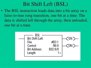
4-bit Shift Register using Xilinx XST and FPGA . EE102 Lab Winter 2005 Electrical Engineering and Computer Science Ohio University. Outline. 4-bit shift register Prototype system: Spartan-3 Sample design overview Lab Procedure Testing Schedule. 4-bit shift register.

E N D
4-bit Shift Register using Xilinx XST and FPGA EE102 Lab Winter 2005 Electrical Engineering and Computer Science Ohio University EE102 EECS Ohio University
Outline • 4-bit shift register • Prototype system: Spartan-3 • Sample design overview • Lab Procedure • Testing • Schedule EE102 EECS Ohio University
4-bit shift register EE102 EECS Ohio University
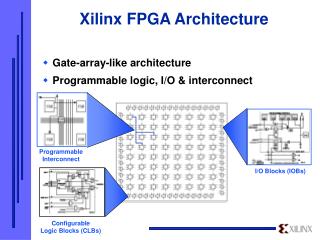
System Board Spartan-3 Flash memory JTAG cable to Parallel port C O N N E C T O R SpartanIIE 200-PQ208 7-S LED 4 push buttons Switch 1-8 8 LEDs Prototype system: Spartan-3 EE102 EECS Ohio University
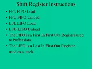
Shiftreg_s3 Shiftreg_final UCF Shiftreg_4 FSM Shiftreg_1 Sample design overview 4-bit shift register: • Reset– button “Btn0” • Preset – button “Btn1” • Clock – button “Btn2” • Input bit – switch 7 • Preset data – switch 3-0 Three functional modules: • 4-bit shift register • Controller controlling the state of reset, load or shift • I/O interface EE102 EECS Ohio University
Procedure 1. Creating project and adding source: EE102 EECS Ohio University
Procedure 2. Creating one-bit register symbol EE102 EECS Ohio University
Procedure 3. Building 4-bit shift register in Schematic Editor EE102 EECS Ohio University
Procedure 3. Building 4-bit shift register in Schematic Editor EE102 EECS Ohio University
Procedure 3. Building 4-bit shift register in Schematic Editor EE102 EECS Ohio University
Procedure 4. Adding design constraints EE102 EECS Ohio University
Procedure 5. Synthesize the design EE102 EECS Ohio University
Procedure 6. Generate the bit programming file EE102 EECS Ohio University
Procedure 7. Download the bit file to FPGA chip EE102 EECS Ohio University
Procedure 8. Test the design EE102 EECS Ohio University
Schedule • Webpage: http://www.ent.ohiou.edu/~webcad/ee102 Please print out the instruction before the lab • Schedule: A01: 03/08 Tuesday 1PM~3PAM A02: 03/10 Thursday 8AM~10AM A03: 03/10 Thursday 1PM~3PM • Rm 306, Stocker Center EE102 EECS Ohio University
Thank you EE102 EECS Ohio University
HDL(Hardware description language) • VHDL: Very high-speed integrated circuits Hardware Description Language– a higher level of abstraction to capture designs. • Xilinx XST: Xilinx Synthesis Tools take these HDLs and automatically translate them into schematics, map them as gates and switches on FPGA chip. EE102 EECS Ohio University