Shift Register
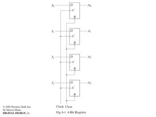
Shift Register. Register. A register is a group of flip-flops, each one of which is capable of storing one bit of information. Issues: You do not have an option hold the output when you don’t want to outputs updated. 4 D flip-flops=4 bits of storage=4-bit register.


Shift Register
E N D
Presentation Transcript
Register • A register is a group of flip-flops, each one of which is capable of storing one bit of information. • Issues: • You do not have an option hold the output when you don’t want to outputs updated. 4 D flip-flops=4 bits of storage=4-bit register
Load=“1”→Update I0 is fed to DFF when Load is a 1. “0” “1” “1” “0” “I0” “I0”
Load=“0”→Hold! A0 is fed to DFF when Load is a 0. So the output is holding! “1” “0” “0” “A0” “A0” “0”
Four Bit Shift Register 1 2 3 4 Q of DFF1 gets SI after the first rising edge of the CLK Q of DFF2 gets SI after the second rising edge of the CLK Q of DFF3 gets SI after the third rising edge of the CLK Q of DFF4 gets SI after the fourth rising edge of the CLK
Serial Transfer Using Shift Register Information in A is made to circulate by connecting SO to SI.
Parallel Transfer Versus Serial Transfer (Serial Transfer) Take multiple clock cycles to transfer data. Assume n=4, each shift Register has 4 DFF. Parallel Transfer Transfer all the bit in one clock cycle. Require combinatorial circuits.
Augend, Addend & Sum 1011 +1001 ______ 10100 Augend Addend Sum
Serial Adder Assuming a shift-right register, the left most position becomes available for storage after the second rising edge of the clock. 1 0 (Augend) 1 1 Feed “1” to z at the next rising edge of the CLK (Addend) Note that The sum can be stored in a third register. But if you want to save shift register, you can store it in A since more and more slots in SRA become available.
Serial Adder At the end of T4 S3 S2S1S0A3 Co D2D1D0B3 A3A2A1A0 B3B2B1B0 ________________ CoS3S2S1S0
Allowing the Serial Adder to Accumulate T3 T2T1T0S3 Ro X2X1X0D3 Co S3 S2 S1S0 D3D2D1D0 ________________ Ro T3 T2 T1 T0
Accumulate with a Shift Register • A, B and D, each represents a 4 bit sequence. • We want to perform A+B+D • Store A in shift register A. • Store B in shift register B. • Allow the CLK to go on for a couple of cycles. • Store the sum bits of A+B in Shift A and allow D to enter shift register B. • Allow more cycles of CLK. • Add D to A+B, and allow A+B+C to enter shift register A.
Block Diagram of a Universal Shift Register This is called the universal shift register because it has both shifts and parallel load capabilities.
S0=0, S1=0 [No Change Mode] S0=0, S1=0
S0=1, S1=0 [Shift Right Mode] S1=0 , S0=1
S0=0, S1=1 [Shift Left Mode] S1=1 , S0=0
S0=1, S1=1 [Parallel Load Mode] S1=1 , S0=1
Breadboard Implementation Universal shift regsiter Random Number Generator
Waveform Random A3 A2 A1 A0 CLK