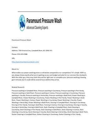
00:00

Understanding Power Amplifiers in Analog Circuits

This chapter focuses on power amplifiers in analog circuits, analyzing circuits that deliver power to loads efficiently while maintaining linearity in the output signal. It discusses power dissipation in transistors, particularly in the output stage, and the importance of managing heat generation. Classifications of power amplifiers based on transistor operation are explored, with a detailed look at Class-B operation including circuit structure, operating principles, and selecting appropriate power BJTs. The chapter also includes an example to illustrate the concepts discussed.

orgilles
Télécharger la présentation

Understanding Power Amplifiers in Analog Circuits

An Image/Link below is provided (as is) to download presentation Download Policy: Content on the Website is provided to you AS IS for your information and personal use and may not be sold / licensed / shared on other websites without getting consent from its author. Content is provided to you AS IS for your information and personal use only. Download presentation by click this link. While downloading, if for some reason you are not able to download a presentation, the publisher may have deleted the file from their server. During download, if you can't get a presentation, the file might be deleted by the publisher.

E N D

Presentation Transcript


  1. Teaching Materials of Analog Circuits Chap 5 Weiwei Xia College of Physics Science and Technology Yangzhou University Yangzhou, 225002 Email: wwxia@yzu.edu.cn

  2. Chapter 5 Power Amplifiers § §5.0 Preview In previous chapters, we dealt mainly with small- signal voltage gains, current gains and impedance ch- aracteristics. In this chapter, we analyze circuits that deliver a specified power to a load. We will therefore, be concerned with power dissipation in transistors, especially in the output stage since the output stage must deliver the signal power. Linearity in the output signal is still a priority.

  3. § §5.0 Preview A multistage amplifier may be required to deliver a large amount of power to a passive load. This power may be in the form of a large current deliv- ered to a relatively small load resistance such as an audio speaker, or may be in the form of a large vol- tage delivered to a relatively large load resistance such as in a switching power supply. The output st- age of the power amplifier must be designed to meet the power requirements.

  4. § §5.0 Preview We will look at the characteristics of power BJTs. Such characteristics include the current, voltage and power ratings of these devices, as well as the safe operating area. The heat generated in these transistors from power dissipation must be removed in order to limit the device temperature to a specified maximum rated value. This maximum device temperature is a function of the thermal resistance between the tran- sisror and the ambient and determines the maximum safe operating power of the transistor.

  5. § §5.0 Preview Power amplifiers are classified according to the percent of time the output transistors are conducting. An often-used output stage for power amplifiers, called a class-AB circuit, uses complementary pairs of transistors. We will analyze several configurations of this type of output stage, One principal goal of this chapter is that the reader will be able to und- erstand the characteristics of a class AB output stage.

  6. § §5.1 The General Problems of Power Amplifiers 一、 一、Characteristics and Object of Study Two important functions of the output stage are to provide a low output resistance so that it can de- liver the signal power to the load without loss of gain and to maintain linearity in the output signal. 1. Po↑ Po PD (5—1) η= — 2. η↑ 3. THD↓ 4. Heat dissipation of BJTs

  7. § §5.1 The General Problems of Power Amplifiers 二、Classes of Power Amplifiers Power amplifiers are classified according to the percent of time the output transistors are conducting, or “turn on.” The four principal classifications are: class A , class B , class AB , and class C . For a sinusoidal input signal. In class—A operation, an out- put transistor is biased at a quiescent current ICQ and conducts for the entire cycle of the input signal. For class—B operation, an output transistor conducts for 二、

  8. § §5.1 The General Problems of Power Amplifiers only one—half of each sine wave input cycle. In class —AB operation, an output transistor is biased at a small quiescent current ICQ and conducts for slightly more than half a cycle, In contaast, in class—C oper- ation, an output transistor conducts for less than half a cycle. These classifications are illustrated in Figure 5.1. ICQ ↓→ η↑

  9. § §5.1 The General Problems of Power Amplifiers iC iC iC iC Q ICQ Q O vCE O O ωt vCE O ωt iC iC Q ICQ O vCE O ωt Figure 5.1

  10. § §5.2 Class—B Operation 一、 一、Circuit Structure 二、 二、Operating Principle 1. Po and Pom +VCC Vom Vom 2 2 RL Vom2 = — · —— 2 RL 1 Vcem2 1 Po= — · ——= — · ——·ζ2 2 RL 2 RL iC1 Po=Vo Io= —— · ——— T1 1 + vi - + vo - iL T2 RL iC2 VCC2 -VCC Vcem VCC Figure 5.2 (5—2) ζ≈ ——

  11. § §5.2 Class—B Operation iC1 iC1 Icm Icm1 Q VCES O Q 2Ic OVCES vCE VCC vCE1 VCES O m Vcem Vcem1 2Vcem iC2 (a) (b) Figure 5.3

  12. § §5.2 Class—B Operation VCC2 2 RL 1 Pom= — · —— (5-3) 2. η and ηmax 1 2 2 VCC2 PD = — π π π RL ∫ π 0 VCCIcmsin ωt dωt = —VCCIcm= —·——ζ Po π PD 4 η= — = — · ζ (5—4) Pom π PD 4 ηm= —— = — ≈78.5% (5—5)

  13. § §5.2 Class—B Operation 三、 三、Selecting the Power BJTs 1. PTm Pom PT PD- 2 2 π 2 -Po 2 1 PT1= PT2= — = ——— =Pom —ζ- - —ζ2 2 - ζ π dPT1 —— d ζ =Pom — - Vom≈0.6VCC ζ≈0.6, dPT1 —— =0 d ζ 2 1 ×0.6- π 2 PT1m= PT2m=Pom —× ×0.62 ≈0.2Pom (5-6) - —×

  14. § §5.2 Class—B Operation VCC2 ( ——) 2RL 1.27 P/ 1.2 PD 1.0 0.8 Po 0.6 PD=Po+2PT1 0.4 PT1 0.2 0.137 O Vom /VCC 0.2 0.4 0.6 0.8 1.0 Figure 5.4

  15. § §5.2 Class—B Operation 2. Selecting the Power BJTs (1) PCM ≥PT1m ≈0.2 Pom (2) │V(BR)CEO │> (3) ICM ≥ VCC/RL Example 5.1: For the circuit shown in figure 5.2. >2VCC Assume that VCC=12V, RL=8Ω, ICM=2A, PCM=5W, │VBR(CEO)│=30V. (1) Determine the value of Pom and examine if the transistors are in safety;

  16. § §5.2 Class—B Operation (2) Determine the value of Po when η=0.6. (1) Pom=9W, ICM=1.5A, PTm=1.8W;VCEM=24V (2) Po≈5.3W. 四、 四、Crossover Distortion Figure 5.5 shows an output stage that consists of a complementary pair of bipolar transistors. When the input voltage is vi=0, both transistors are cutoff

  17. § §5.2 Class—B Operation and the output voltage is vo=0, If we assume a B-E cut-in voltage of 0.6V, then the output voltage vO re- mains zero as long as the input voltage is in the ra- nge -0.6V ≤ vi ≤0.6V . There is a range of input voltage around zero volts where both transistors are cutoff and vo is zero. This portion of the curve is called the dead band, and it produces a crossover distortion. As shown in Figure 5.6.

  18. § §5.2 Class—B Operation +VCC vi/V 0.6V ωt 0 -0.6V T1 vo vi vO,iL iL T2 RL 0 ωt -VCC Crossover Distortion Figure 5.5 Figure 5.6

  19. § §5.3 Class—AB Push-Pull Complementary Output Stages A class –AB output stage eliminates the cross- over distortion in a class –B circuit, we will analyze several circuits that provide a small quiescent bais to the output transistors. Such circuits are used as the output stage of power amplifiers, as well as the output stage of operational amplifiers, and will be discussed in Chapter 6. 一、 一、Class –AB Output Stage with Diode Biasing

  20. § §5.3 Class—AB Push-Pull Complementary Output Stages +VCC +VCC RE3 RE3 iC1 iC1 vi vi T3 T3 T1 T1 R1 D1 D2 vo T4 vo iL iL R2 T2 RL T2 RL RC3 RC3 iC2 iC2 -VCC -VCC Figure 5.7 Figure 5.8

  21. § §5.3 Class—AB Push-Pull Complementary Output Stages 二、 二、Class –AB Biasing Using the VBEMultiplier An alternative biasing scheme, which provides more flexibility in the design of the output stage, is shown in Figure 5.8. If we neglect the base current in T4 , then VBE4 IR2= —— R2 and voltage VCE4 is R1 R2 VCE4= IR2(R1+R2) =VBE4 ( 1+— )

  22. § §5.3 Class—AB Push-Pull Complementary Output Stages Since voltage VB1-B2 is a multiplication of the junction voltage VBE1, the circuit is called a VBEmu- ltiplier. The multiplication factor can be designed to yield the required value of VB1-B2. 三、 三、Class –AB Output Stage Utilizing the Darling- ton Configuration The complementary push-pull output stage uses NPN and PNP bipolar transistors.Usually in IC design, the PNP transistors are fabricated as latreal devices

  23. § §5.3 Class—AB Push-Pull Complementary Output Stages with low β values that are typically in the range of 5 to 10, and the the NPN transistors are fabricated as vertical devices with β values on the order of 200 . This means that the NPN and PNP transistors are not well matched. as we have assumed in our analyses. In Figure 5.9, the output stage uses Darlington pairs. Transistors T1and T2constitute the NPN Dar- lington emitter - follower that sources current to the load. Transistors T3, T4and T5constitute a composite

  24. § §5.3 Class—AB Push-Pull Complementary Output Stages PNP Darlington emitter-follower that sinks current from the load. The three diodes D1, D2and D3est- ablish the quiescent bias for the output transistors. The effective current gain of the three-transistor configuration T3- T4- T5is essentially the product of the three individual gains. With the low current gain of the PNP device T3 , the overall current gain of the T3- T4- T5 configuration is smiliar to that of the T1– T2 pair.

  25. § §5.3 Class—AB Push-Pull Complementary Output Stages +VCC RE6 vi T6 NPN T1 T2 D1 D2 vo iL D3 RL T3 T4 T5 RC6 PNP -VCC Figure 5.9

  26. § §5.3 Class—AB Push-Pull Complementary Output Stages 四、 四、Class –AB Output Stage Using Single Source +VCC +VCC /2 RC3 RC3 T1 T1 vo D1 C K D1 vo + D2 D2 T2 RL vi T2 vi RL T3 T3 - -VCC /2 (b) (a) Figure 5.10 OTL (Output Transformerless )

  27. § §5.3 Class—AB Push-Pull Complementary Output Stages VK=VCC/2 1 C>(5~10) ——— 2πfLRL 1 VCC2 8 RL Pom= — · —— (5—7)

  28. § §5.3 Class—AB Push-Pull Complementary Output Stages 五、 五、BTL (Balanced Transformerless ) +VCC vi>0, T1√ ,T4√ T2× × ,T3× × T1 T3 vi<0, T2√ ,T3√ vo + - T1× × ,T4× × RL + T2 T4 vi VCC2 2 RL 1 Pom= — · —— - Figure 5.11 BTL

  29. § §5.4 Integrated Power Amplifier 一、 一、 SHM1150Ⅱ Ⅱ 6 +VCC 1 + vi - VCC ±12V~ ±50V 8 SHM1150Ⅱ vo Pom=150W 3 10 - VEE Figure 5.12 (a)

  30. § §5.4 Integrated Power Amplifier +VCC 6 R8 R7 R6 T4 T5 T7 T8 C R11 R9 8 1 Rf T6 + vo - T1 T2 R13 + vi - R10 R1 R2 T9 T10 I1 I2 R12 -VEE 10 3 Figure 5.12 (b)

  31. § §5.4 Integrated Power Amplifier 二、 二、 LM386 6 +VCC R2 T8 7 1 8 D1 R3 5 R5 R6 R4 vo 2 3 T2 D2 T1 T4 T3 T9 T10 R1 R7 T7 T6 T5 4 Figure 5.13

  32. § §5.5 Power Transistors Since we are now discussing power amplifiers, we must be concerned with transistor limitations, The limitations involve: maximum rated current ( on the order of amperes), maximum rated voltage ( on the order of 100V), and maximum rated power ( on the order of watts or tens of watts ) , we will consider these effects in the BJT and then in the MOSFET. § §5.5 .1 Power BJTs 、Heat Dissipation of BJTs 一 一 、

  33. § §5.4 Power Transistors The maximum power limitation is related to the maximum allowed temperature of the transistor, which in turn is a function of the rate at which heat is removed. Figure 5.14

  34. § §5.4 Power Transistors (a) (b) Figure 5.15

  35. § §5.4 Power Transistors 1. RT ( oC/W oC/mW ) RT ↓→ PCM↑ RT ↑ → PCM ↓ 2. Heat Dissipation Equivalent Circuit RTj RTc RTf Tj Tf Tc Ta RT ≈RTj +RTc +RTf RT PC 0.1~3 oC/W Figure 5.16 3. Tj- -Ta= RTPCM (5—8)

  36. § §5.4 Power Transistors Tj- -Ta PCM = (5—9) RT RT↓→PCM↑; Ta↓ → PCM↑ . Example 5.2: For the circuit shown in figure 5.16. Assume that RTj=4oC/W, RTc=1oC/W, RTf=5oC/W. The average current IC=1A when C-E voltage VCE=10V. Determine the value of Tj, Tc, and Tf when Ta=25oC. Soluiton: PC=VCEIC=10× ×1=10W Tj=Ta+PC(RTj+RTc+RTf) = 25oC+10W× =125oC ×(4oC/W+1oC/W+5oC/W) Tc=Ta+PC(RTc+RTf) = 25oC+10W× ×(1oC/W+5oC/W)=85oC

  37. § §5.4 Power Transistors Tf=Ta+PCRTf= 25oC+10W× ×5oC/W=75oC 、Second Breakbown 二 二 、 1. Another breakdown effect is called second break- down,which occurs in a BJT operating at high voltage and a fairly high current. Slight nonuniformities in current density produce local regions of increased heating that decreases the resistance of the semicon- ductor material, which in turn increases the current in those regions. This effect results in positive feed-

  38. § §5.4 Power Transistors back, and the current continues to increase, produc- ing a further increase in temperature, until the semi- conductor material may actually melt, creating a short circuit between the collector and emitter and producing a permanent failure. iC C iC B A vCE o o vCE Figure 5.17 Figure 5.18

  39. § §5.4 Power Transistors 2. Safe Operating Area of Power BJTs iC ICM PCM V ≤ 80% V(BR)CEO I ≤ 80% ICM P ≤ 50%PCM T ≤(70%~ 80%) Tj second breakdown Safe Operating Area o V(BR)CEO vCE Figure 5.19 § §5.5 .2 Power MOSFET

  40. § §5.4 Power Transistors s g s metal N+ N+ P N- -layer SiO2 N+ substrate d Figure 5.20

  41. Summary 1. In this chapter, we analyzed amplifiers and out- put stages capable of delivering a substantial amount of power to a load. 2. The maximum power rating of a transistor is re- lated to the maximum allowed device temperature at which the device can operate without being damage. 3. In a class-A amplifier, the output transistor con- ducts 100 percent of the time. The theoretical max- imum power conversion efficiency for a standard class-A amplifier is 25 percent. This efficiency can be theoretically increased to 50 percent by incorporating

  42. Summary inductor or transformers in the class-A circuit. 4. class-B output stages are composed of comp- lementary pairs of transistor operating in a push-pull manner. In an ideal class-B operation , each output transistor conducts 50 percent of the time. For an idealized class-B output stage, the theoretical max- imum power conversion efficiency is 78.5 percent. However, practical class-B output stages tend to su- ffer from crossover distortion effects when the output is in the vicinity of zero volts.

  43. Summary 5. The class-AB output stage is similar to the class-B circuit, except that each output transistor is provided with a small quiescent bias and conducts more than 50 percent of the time. the power con- version efficiency of a class-AB output stage is less than that of the ideal class-B circuit, but is substan- tially large than that of the class-A circuit. Example 5.3:For the circuit shown in figure 5.21.Vi=1V. △vC3/△vB3=-16. Determine the value of Po, PD, PT and η.

  44. Problem Solution: +VCC +24V Vo2 (16Vi )2 Po= — = ——— =16W RL RL R1 T1 D1 vo 2 VCC2 2 VCC2Vom PD = —·——ζ= —·——·—— π RL π RL 2 24× ×16 2 = ——× ×———— ≈21.6W 3.14 16 D2 VCC T2 RL 16Ω vi T3 R2 -VCC -24V PT =PD- -Po=21.6-16=5.6W Figure 5.21 Po PD 21.6 16 η= — × ×100%= —— × ×100%≈74.1%

  45. Problem Example 5.4: Yang P165Problem 6-8 -VCC -12V RB1 680Ω Tr1 Tr2 T1 + N1 100 RL 8Ω N2 100 vi N1 100 - - T2 RB2 10Ω Figure 5.22

  46. Problem VCC2 1 122 2 RL′ 2 8 1 Solution: (1) Poc= — · —— = — × × — =9W N1 N2 2 Where: RL′= — RL= 8Ω Po= PocηT=9× ×0.8=7.2W 2 VCC2 π RL′ 3.14 8 2 122 × — =11.5W PD= — · —— = —— × Po PD 11.5 7.2 η= — × ×100%= —— × ×100%≈62.6%

  47. Problem VCC RL′ 12 (2) ICM= —— = — =1.5A 8 │VCEM│=2VCC=24V PD= Po+ PT PT= PD- - Po 1 1 -Po)= ─× 2 2 PT1= PT2= ─ (PD- ×(11.5 - -9)=1.25W

More Related